¶ Free Electron Theory
The Free Electron Theory provides a successful and simplified departure from the traditional chemical perspective of overlapping orbitals
- Several key assumptions underlie this model :
- Only valence electrons can move freely, while core electrons, deeply held by ions, remain stationary.
- The model disregards forces between free electrons, a simplification known as the independent electron approximation.
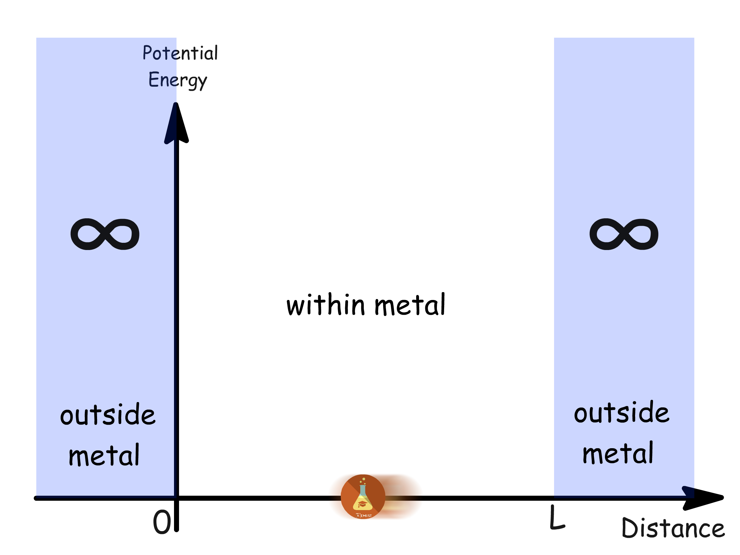
- Positive ions are smeared into a continuum of positive charge, creating an environment where electrons move freely within a constant potential
Building upon these assumptions, the model employs a hypothetical "particle in a box" scenario to represent the system
- We envision a cubic macroscopic metal lump with a side length that defines the size of the box
- The independent electron assumption enables the calculation of wavefunctions and eigenvalues for one conduction electron, treating other electrons as if absent
- The resulting energy levels calculated from one electron are then populated using the Pauli Exclusion Principle
¶ k-space
The confinement within the metal box results in quantization of the wavevector , which in turns results in quantization of energy levels
- , and are the quantum numbers that define the system and they can only take integer values
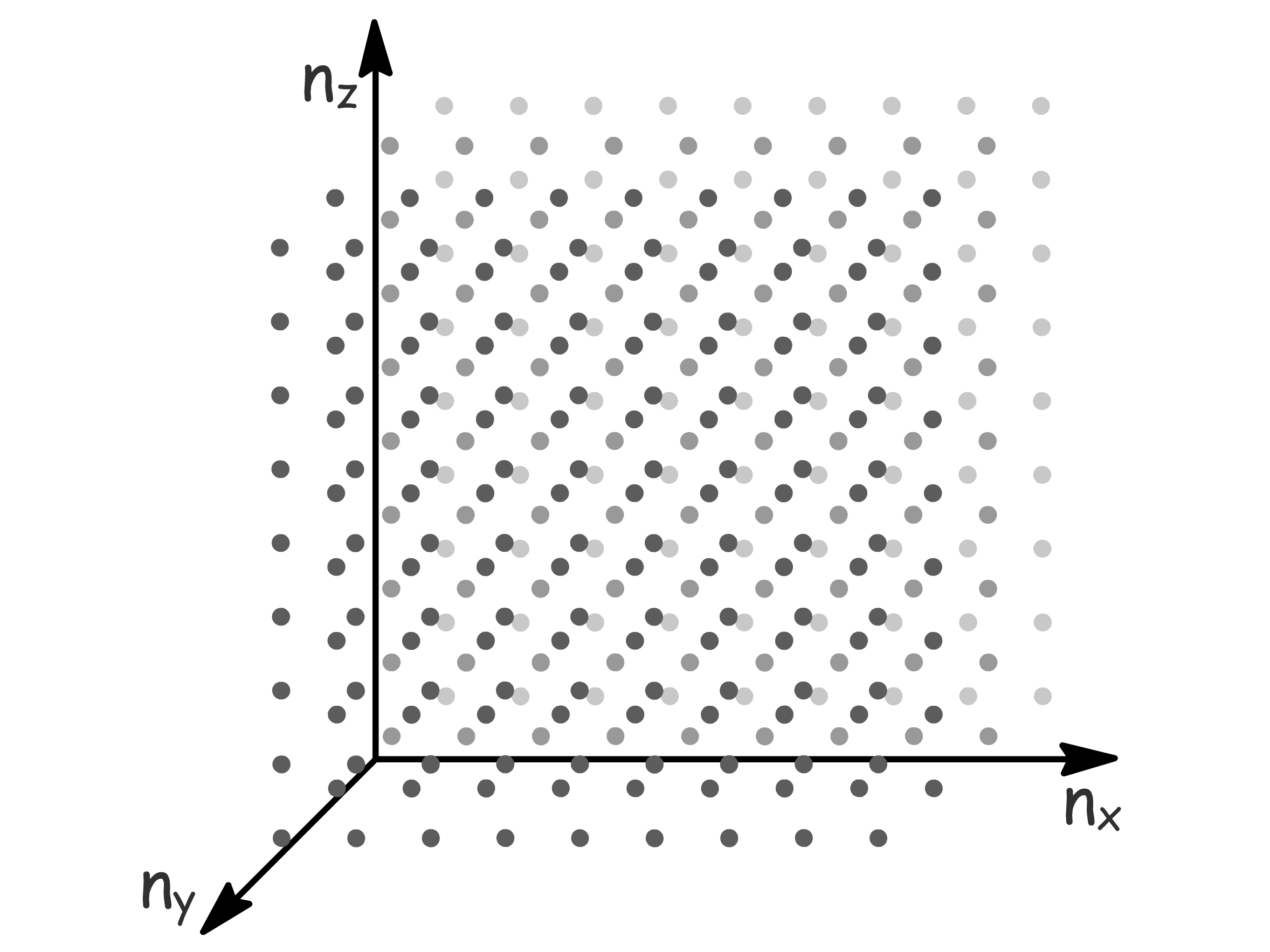
It is convenient to represent the different energy levels in a graphical way by thinking of each combination of quantum number as a point in a cubic lattice
- Such a space is called the -space
- If the spacing of points in the imaginary lattice is one unit, the point representing a particular state is found at a distance from the origin given by
- Thus all points in the lattice with the same distance from the origin represents degenerate energy levels
The energy of the highest occupied state is called the Fermi Energy and we shall derive an expression for it
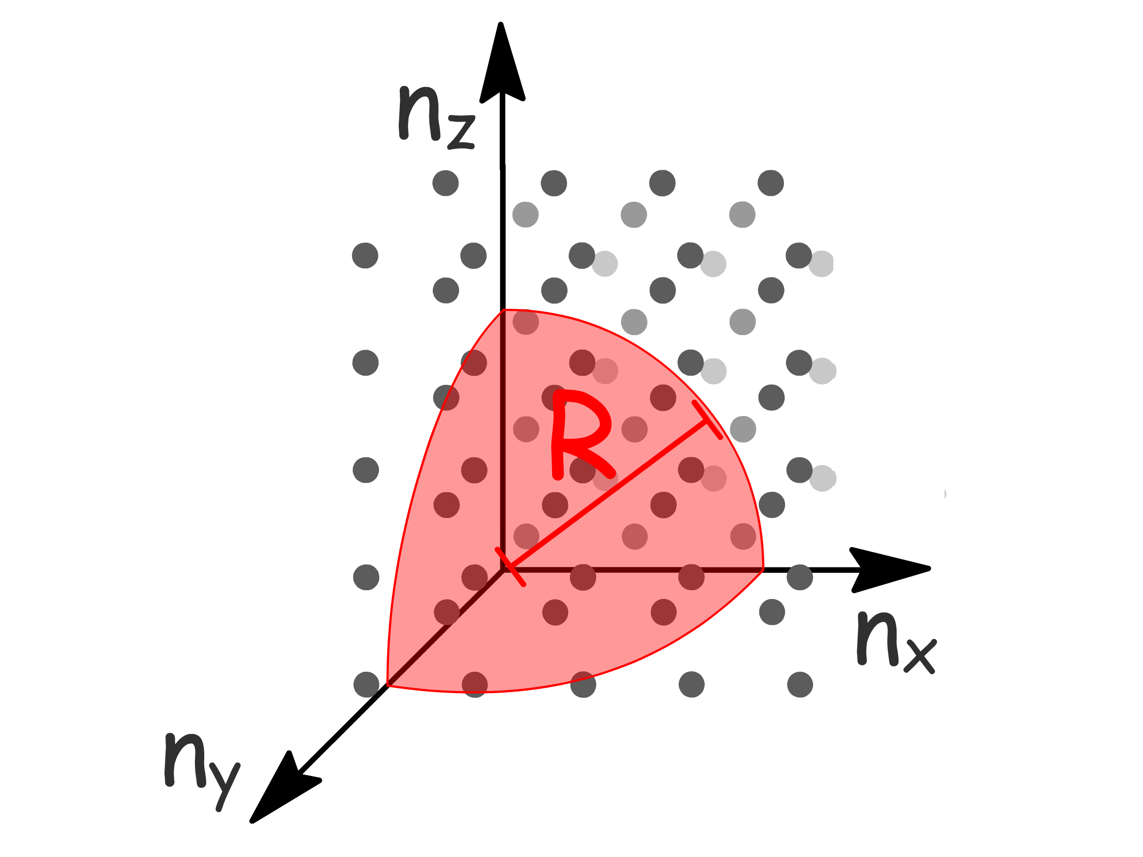
- Since only positive values of are allowed, the number of orbitals below can be found by counting the points inside the positive octant of a sphere of radius
- Since the distance between the points is 1, the number of points within the octant is simply the volume of the octant
- The Pauli Exclusion Principle tells us that the total number of electrons ( ) is twice that of the orbitals
- Expressing it in terms of
- is just the volume of the box, so is equal to the density of electrons
- Similarly, we can also derive any expression for the Fermi wavevector
Note that since is very large, the energy difference between successive eigenvalues become successively small
- Therefore the quantization condition on is not very signidicant and its main use is that it enables to keep track of the number of eigenstates in a region of k space
¶ Distribution of Electrons
Density of Available States
The distribution of available orbitals in a material is not uniform across all energy levels
- Some energy levels may have a concentration of more degenerate orbitals
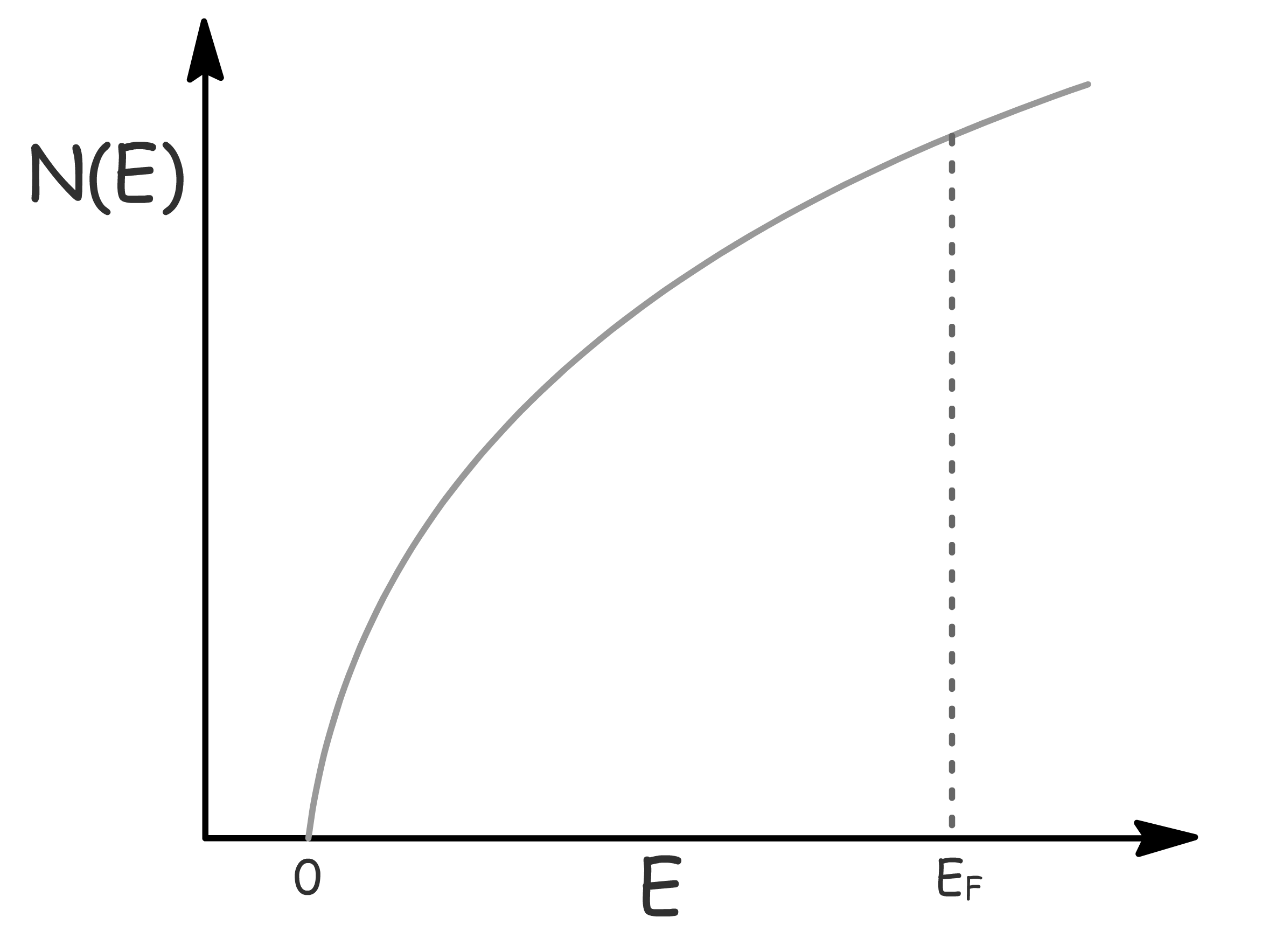
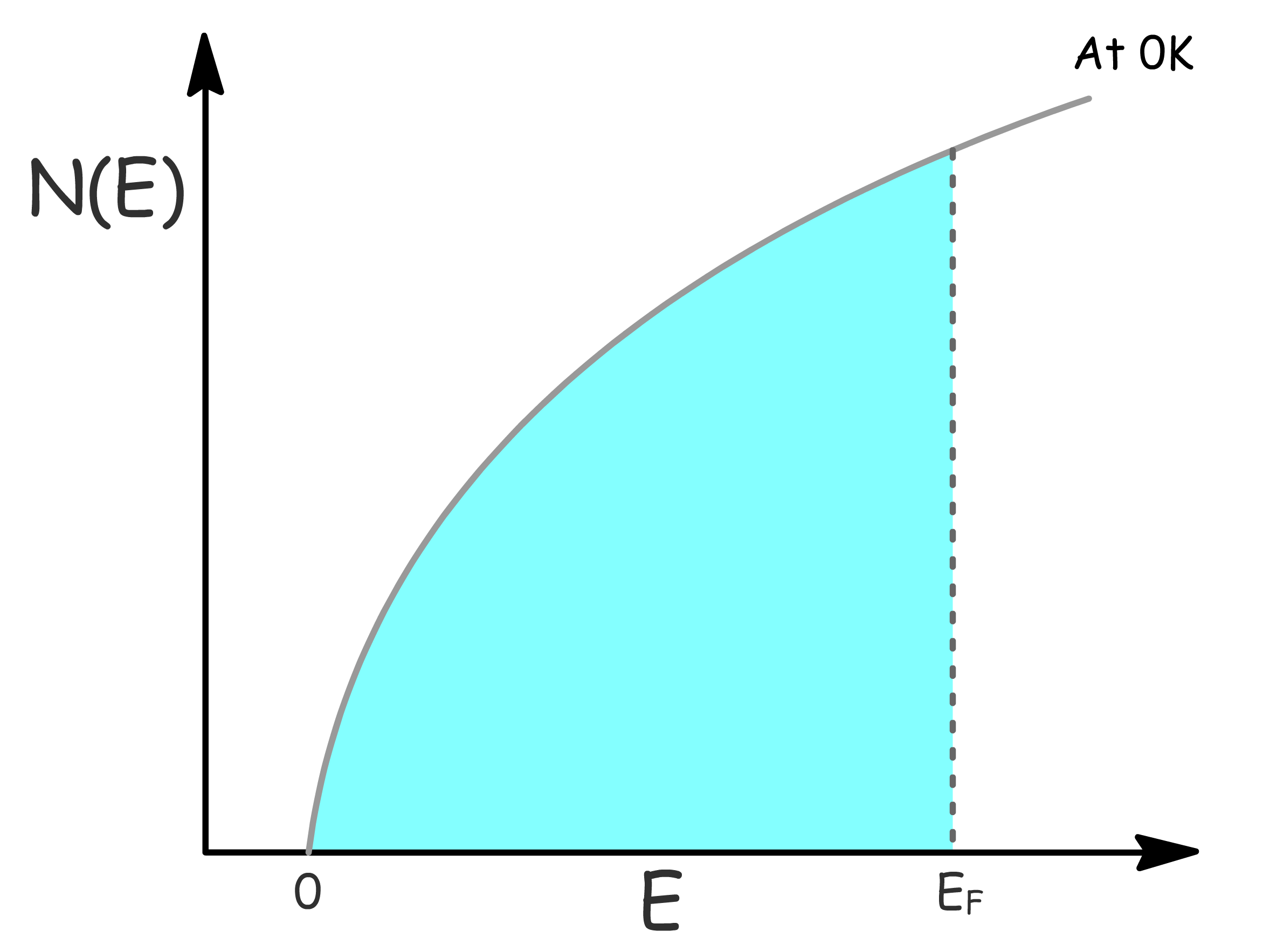
To quantitatively describe the distribution of these energy levels, we introduce the concept of the density of available states, denoted as
- represents the number of available energy levels with an energy of per unit volume
- Mathematically, we can define it as
- Plotting this function provides insight into the distribution of energy levels
Fermi-Dirac distribution
The Fermi-Dirac distribution, , describes the probability that an electron will occupy a state at a finite temperature
- At , is 1 for , but 0 for and at E = E_
- With increasing temperature, the probability of electrons occupying energy levels of increases, resulting in a broadening of the distribution
We can generalize the initial definition of Fermi Energy to temperatures beyond absolute zero
- Formally, the Fermi-level, as defined by the Fermi-Dirac distribution, is the energy at which the probability of occupancy is \frac{1}
- This is a characteristic that holds true at any temperature
The Fermi-Dirac distribution serves as the counterpart to the Boltzmann distribution, specifically tailored for fermions within a band of states
- For , reduces to the classical Boltzmann distribution
- This explains why the 'tail' of the distribution at elevated temperatures closely resembles the Boltzmann distribution
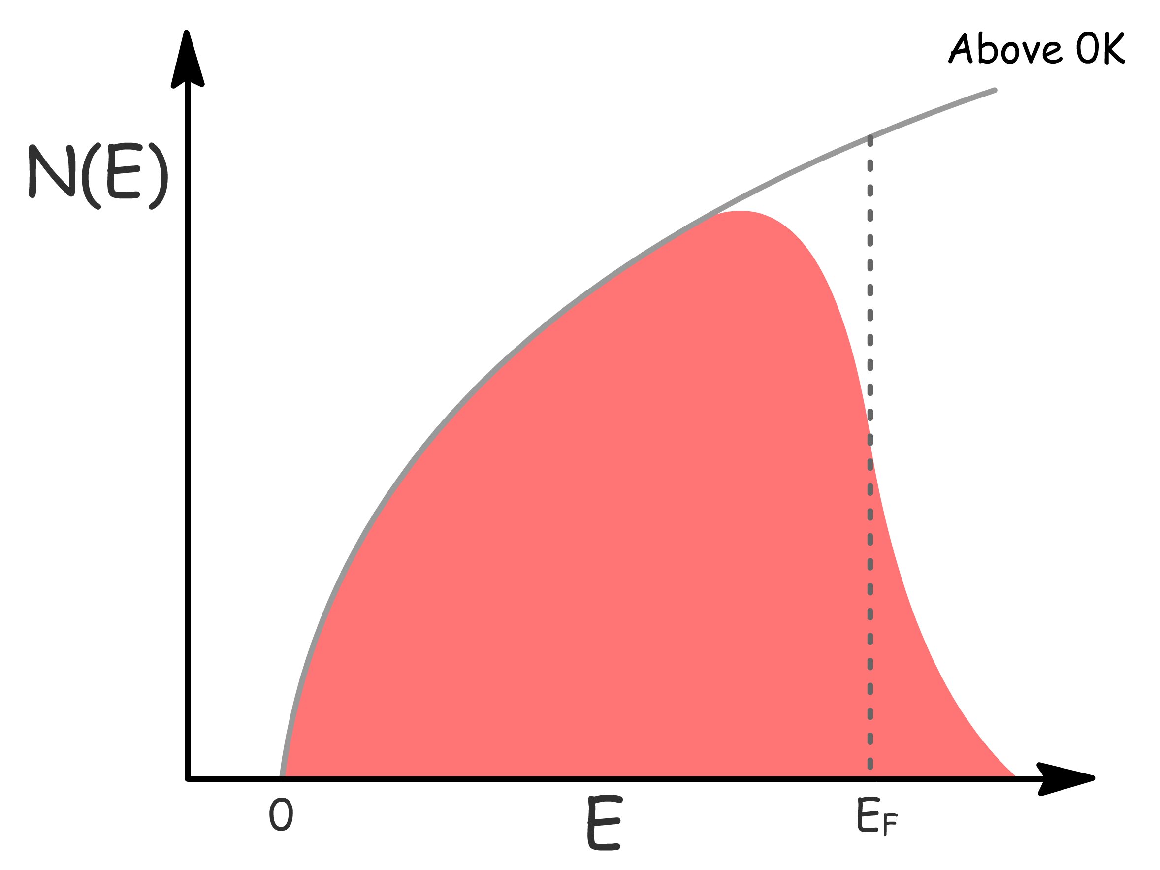
Density of Occupied States
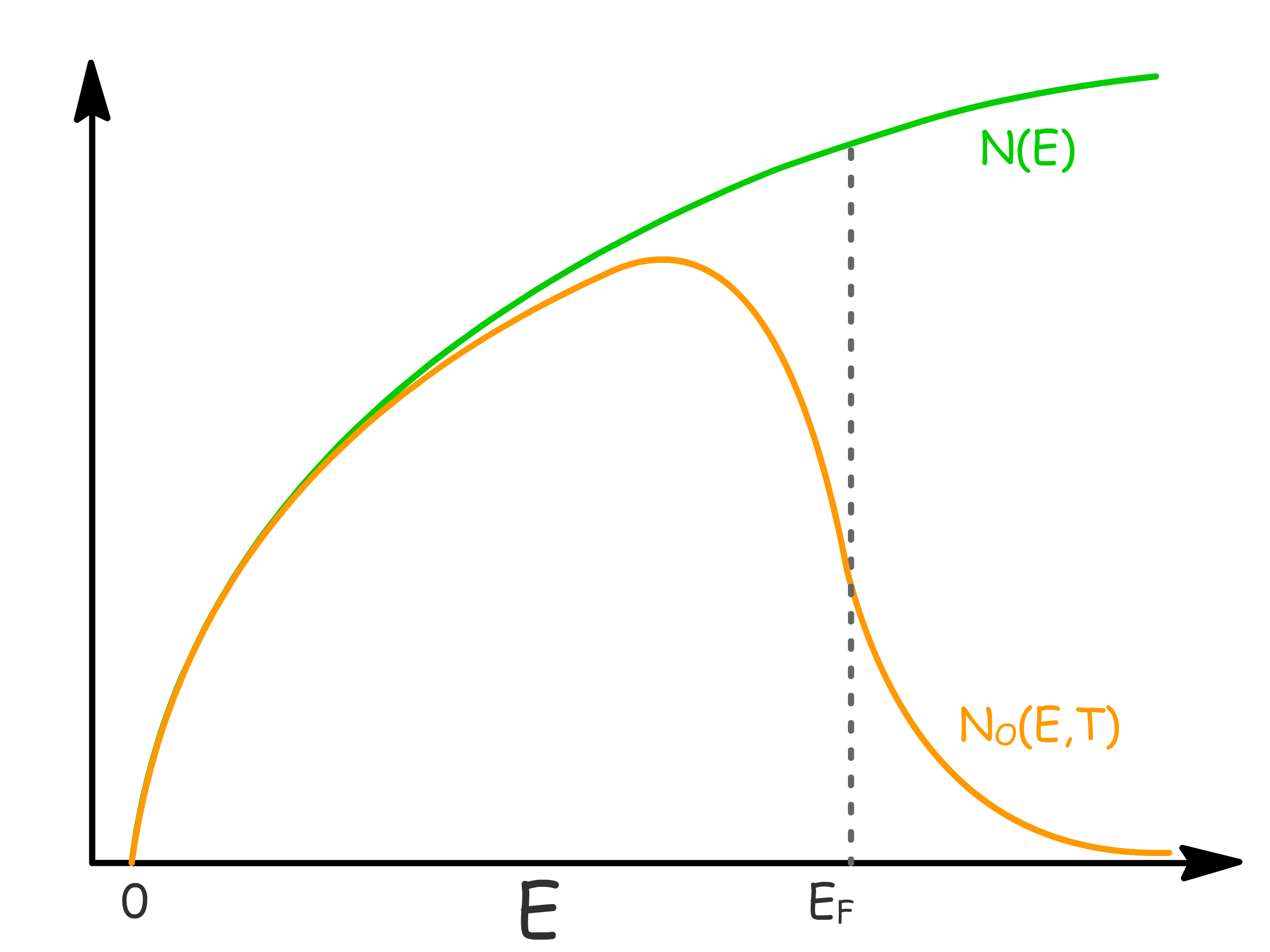
Having constructed how available energy levels are distributed and how electrons are distributed at different energy and temperature, we are now in a position to devise the density of occupied states
- is the number of occupied orbitals of energy at temperature
- Mathematically, it is defined as the product of the density of available states and the Fermi-Dirac distribution
- Often we approximate electrons are only excited from occupied states into unoccupied states within a range of from .
Effect of an Electric Field on Occupancy of States
Recall that conduction fundamentally arises from the net movement of electrons
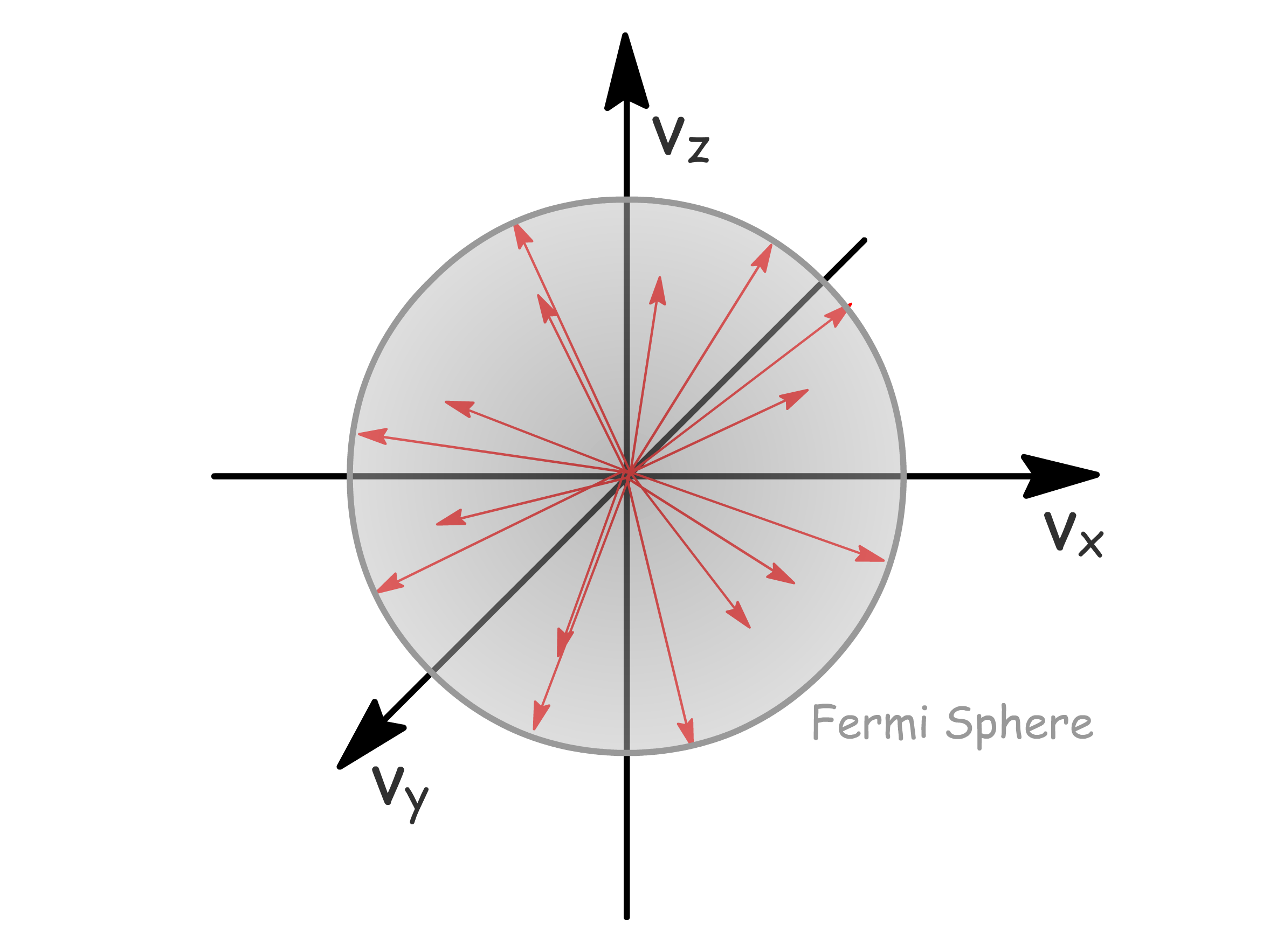
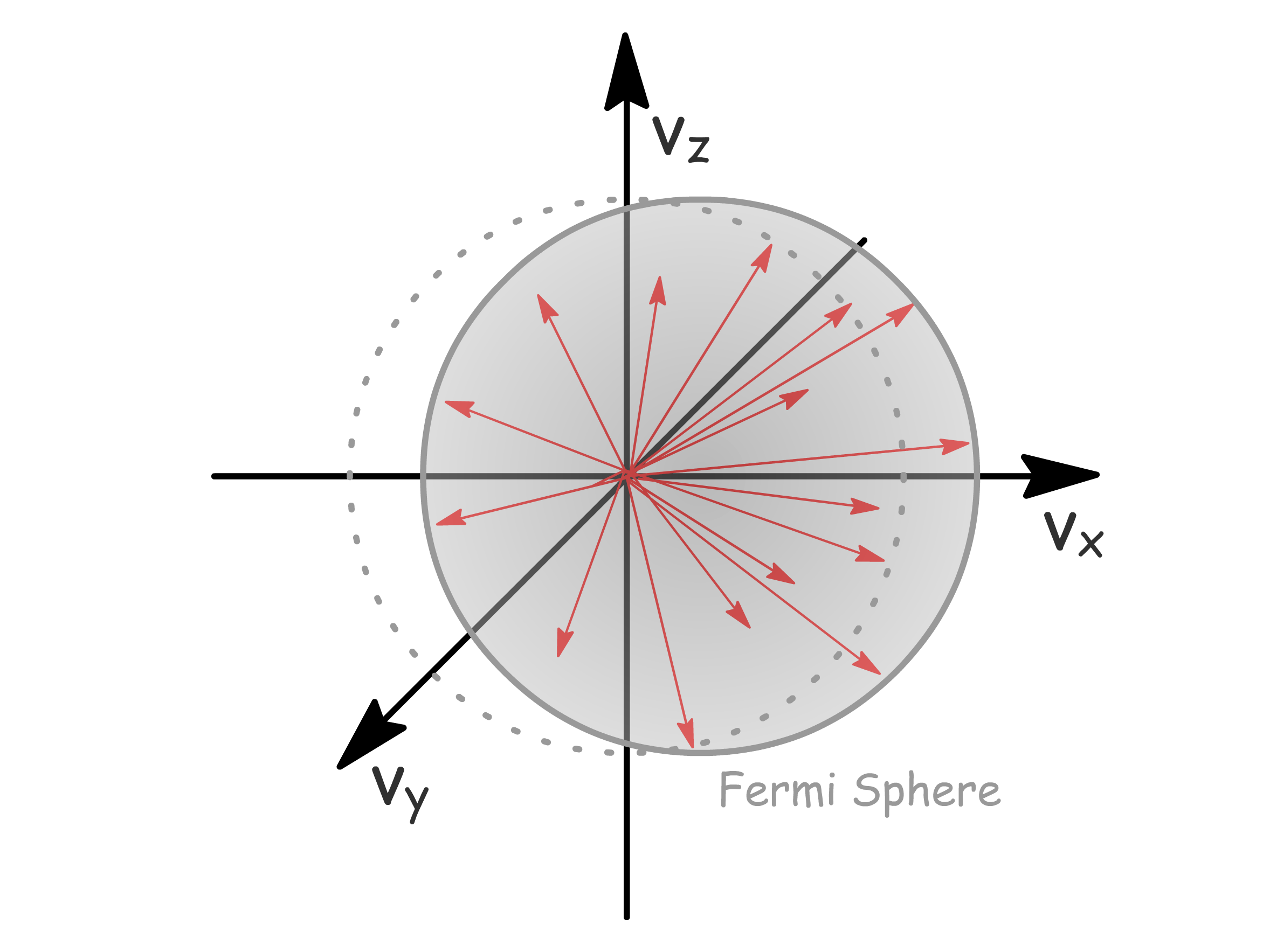
- To delve into the electron motion, let's transition our viewpoint from -space to velocity space
- However, given the indirect relationships ( ) and ( ) between and velocity via momentum, this spatial shift is essentially a rescaling process
- In simpler terms, there is no substantial qualitative distinction between the two spaces
The conduction property of solid emerges as a result of an external electric field
- In the absence of an external field, the Fermi sphere exhibits symmetry since electrons move in random directions with random velocities, resulting in an average velocity over the sphere of 0. Consequently, there is no net conduction
- The introduction of an external field induces an energy shift in electrons, moving them from states below in one direction to states above in another. This shift facilitates net electron motion (conduction) and gives rise to an asymmetric Fermi sphere
- Notably, the effectiveness of this process relies on the presence of unoccupied states above
¶ Other Theories and Band Structure
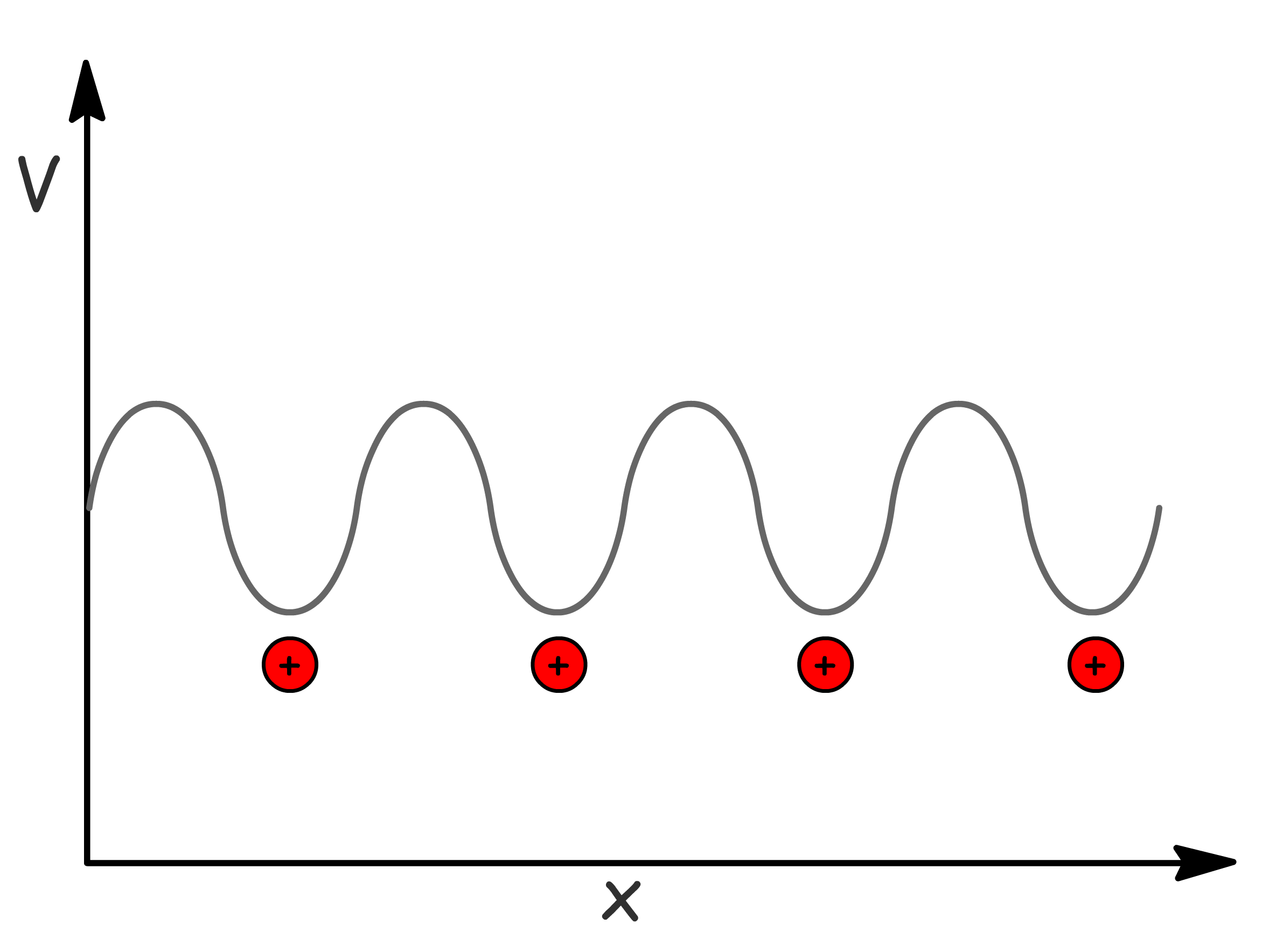
In the following two models, we will adopt an assumption of a periodic potential described by the equation
- The potential is at its minimum when in proximity to the nuclei, as illustrated in the figure below
Bloch's Theorem
Since the potential is periodic, the solution to the differential equation must satisfy Bloch's theorem
- Bloch's theorem states that solutions to the Schrödinger equation in a periodic potential can be expressed as plane waves modulated by periodic functions
- is the plane wave, is another periodic function with the periodicity of the lattice where
- Bloch's theorem implies that the behavior of electrons in a crystal is determined by the interaction with the periodic potential of the crystal lattice
¶ Crystal-Orbital Theory
We treat crystal orbitals using LCAO approach and uses translational symmetry (due to unit cells) of the lattice to simplify them
- The atomic orbitals on each atom now forms the periodic function in the Bloch function
- Interesting phenomena arise when we consider the situation of and , where
- Their difference will be apparent once we expand the summation
So far we have yet specify which atomic orbital is used
- Suppose is the orbital for the atom
- Suppose is the orbital for the atom
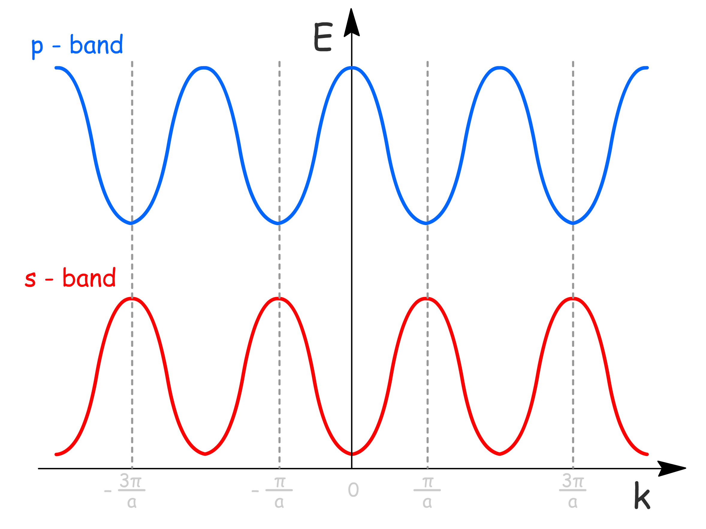
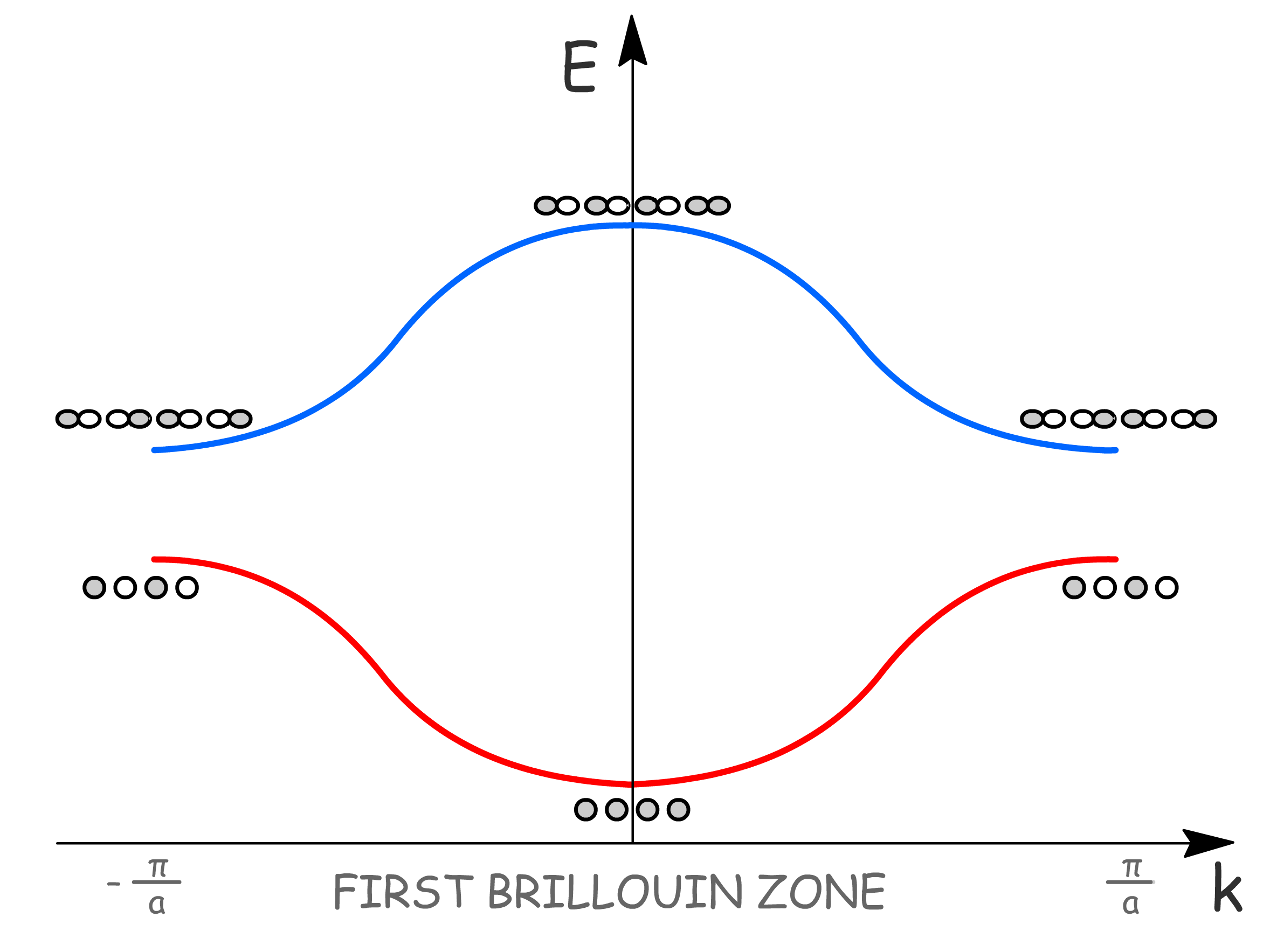
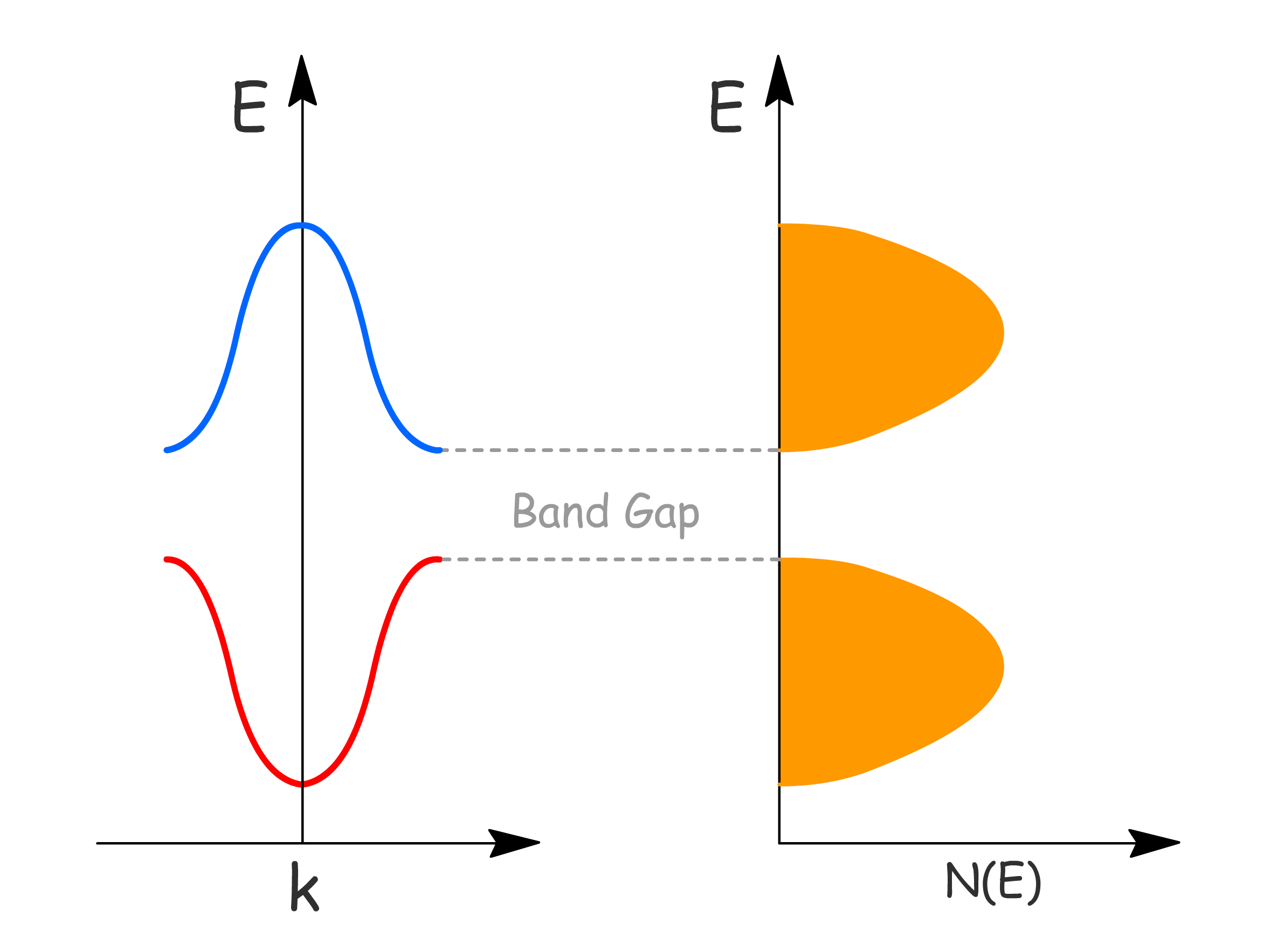
and are the two ends of the extremes, we can in fact plot out how energies vary with values
- Due to the periodic nature of the lattice, we only need to plot in that rangeto obtain all the information we need. By convention, the chosen range is and is called the first Brillouin zone
- Moreover, since here is introduced as a quantum number, it is necessary to limit its value to , so as not to duplicate crystal orbitals
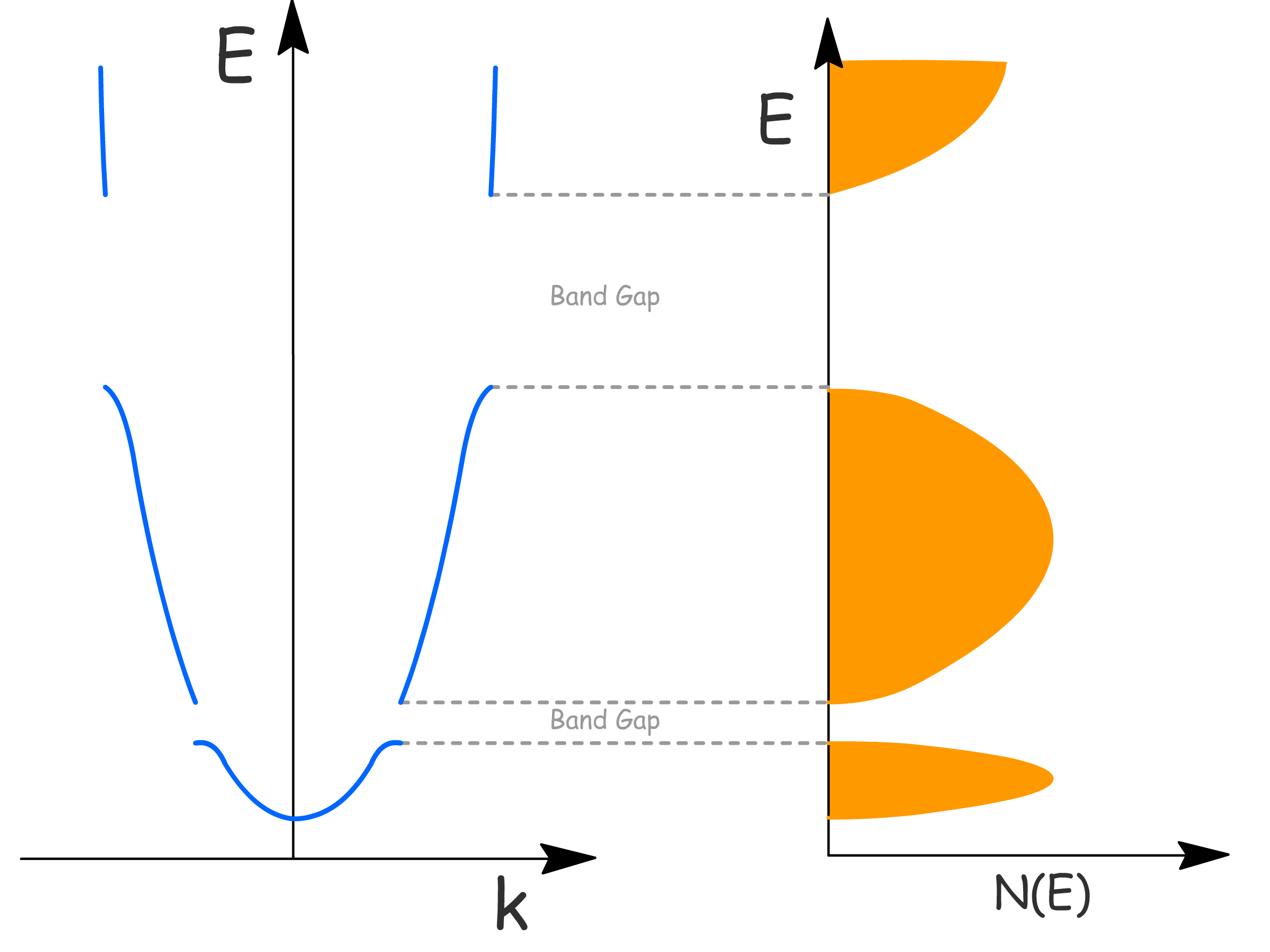
- We can see that there is region of energy values that do not have a corresponding orbital
- The range of (band dispersion) depends on the strength of neighboring AO interactions ()
Extension to Two Dimensions
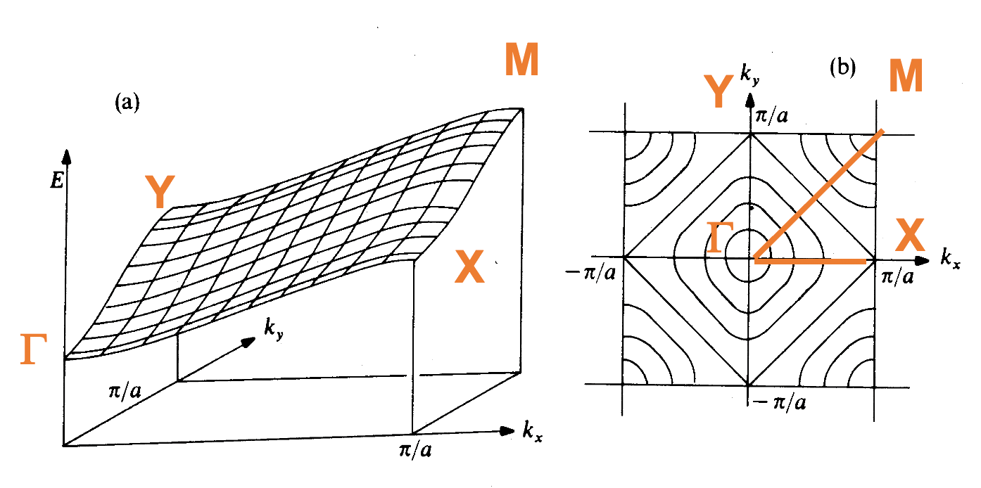
In 2D, we have and and their values are independent of each other
- The Bloch Function in 2D for this model is now
- And the wavelength in terms of is
The extra dimension allows for bonding and antibonding interactions to happen at the same time
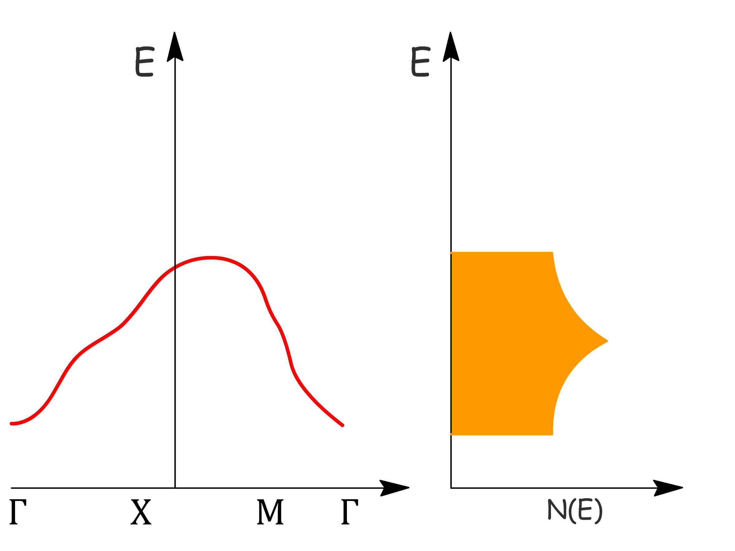
- Therefore there are a unique set of values in the range
- In the band, (The opposite is true for the band)
As is proportional to the inverse slope of the bands
- Steep bands (large overlap) correspond to a small , and flat bands (small overlap) correspond to a large
¶ Nearly-Free Electron Theory
As the name suggests, we employ the same solutions from the Free-Electron Theory to the Nearly-Free Electron Theory
- The corresponding energy is therefore given by
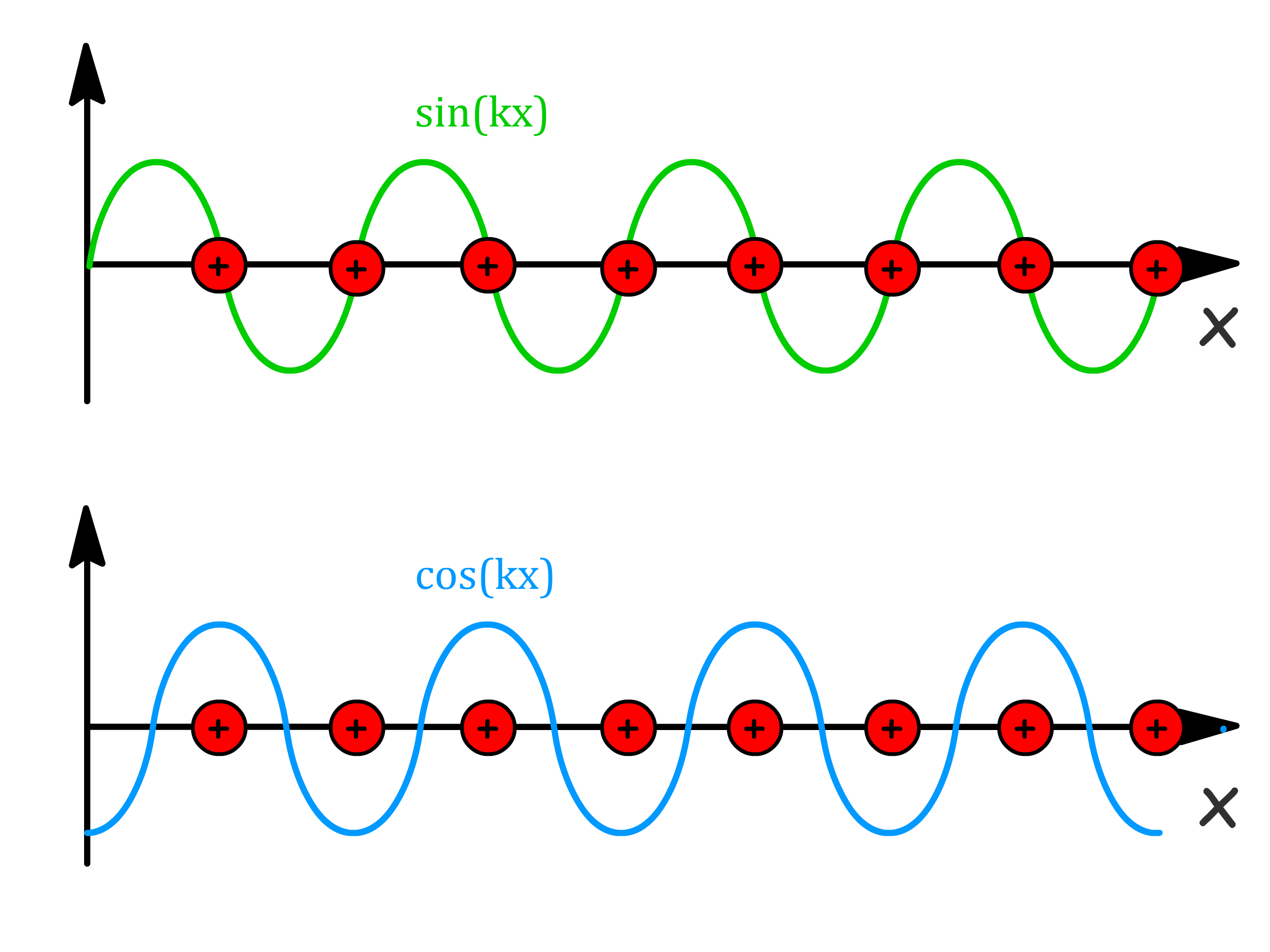
We can express the wavefunction in terms of sine and cosine functions using Euler's theorem
- Interesting phenomena arise when one consider the wavefunction at , where is an integer
- At these k values, the cosine function has its maximum electron density at the atomic positions, whereas the sine function has has zero electron density there
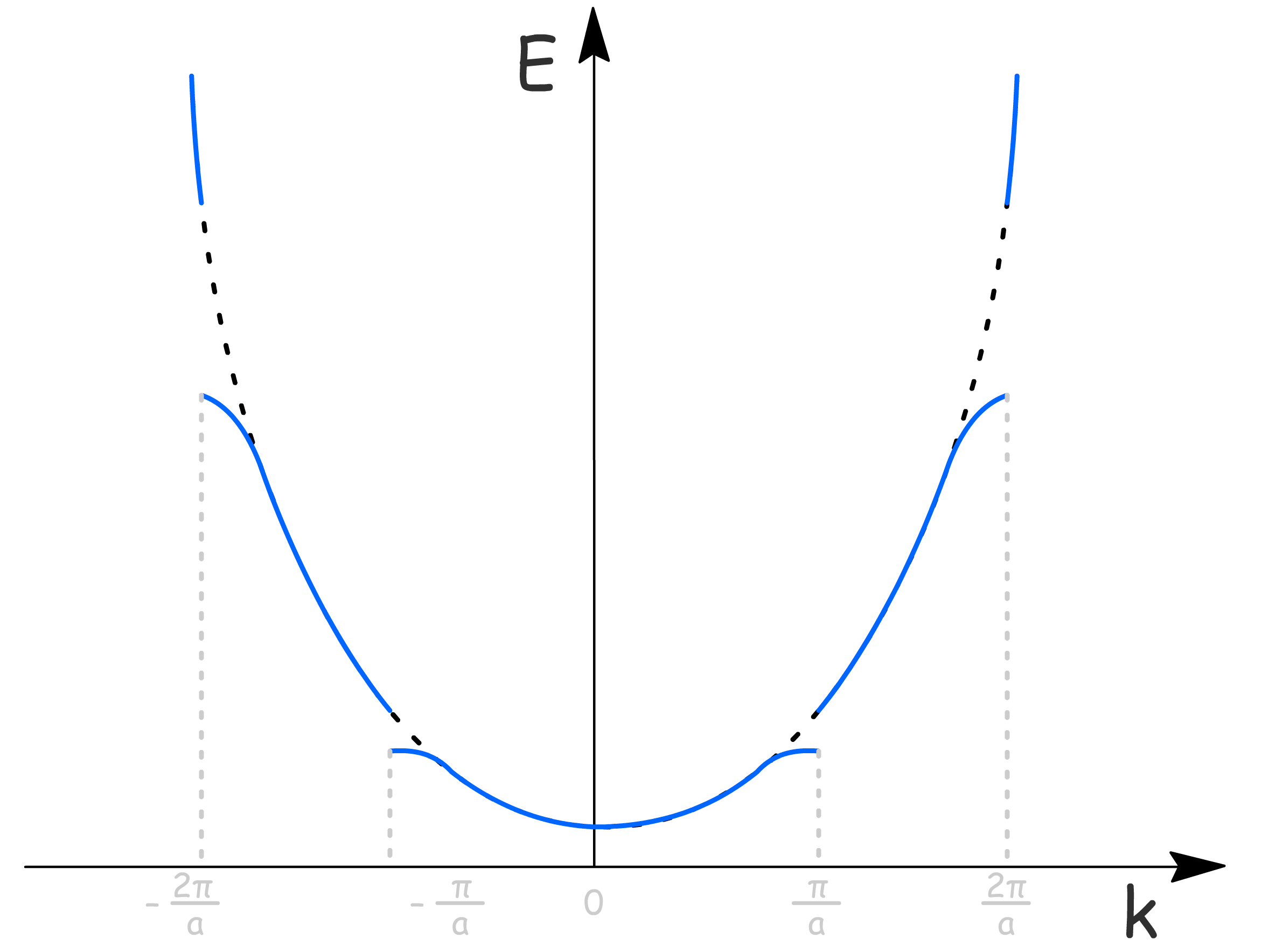
We can then plot the energy against
- The dashed curve is the parabola given by for electrons at constant potential
- The effect of the periodic potential is given by the blue curve, where the splitting at is the energy difference between the sine and cosine function
We can think of the energy gaps in this model as being due to the strong interference of some electron wave in the lattice
- In fact, the corresponding wavelengths are those that satisfy the Bragg condition for diffraction of electrons by the lattice
- Bragg reflection as destructive interference occurs at as back-reflected waves appear, leading to forbidden zones with no states of a particular energy. The two waves have the same kinetic energy due to the same value, but different potential energies
- In this interpretation, the Brillouin zone boundary corresponds to the electron wavelength that satisfies Bragg condition
¶ Comparison of the Models
Assumptions
Crystal orbital theory assumes a strong periodic potential
- Electrons are more likely to be localized around nuclei in this situation
- This localization is crucial for the formation of distinct molecular orbitals associated with individual atoms or molecular groups
The nearly free electron model works best when the overlap is strong
- Atomic orbitals tend to lose their identities in this situation
- As a result, they behave more like free electrons
Band Gap
Crystal Orbital Theory
- Provides a chemical description where the band gaps arise from the energy difference between different atomic orbitals, or between bonding and antibonding combinations
- Band energy width determined by strength of atomic orbital interactions
The Nearly-Free Electron Theory
- Suggests that band gaps come from the interaction of free electrons with the periodic potential in a lattice
- Band energy width determined by \frac{\hbar^2 k^2}
Different Orbitals
Crystal Orbital Theory states that different LCAO are differentiated by different phases of atomic orbital combinations
- The Nearly-Free Electron Theory states that travelling waves are differentiated by different kinetic energies
Applications
- Crystal Orbital Theory is most appropriate for covalent bonding with strong couplings between atoms
- The Nearly-Free Electron Theory is most appropriate for metallic bonding
¶ Semiconductors
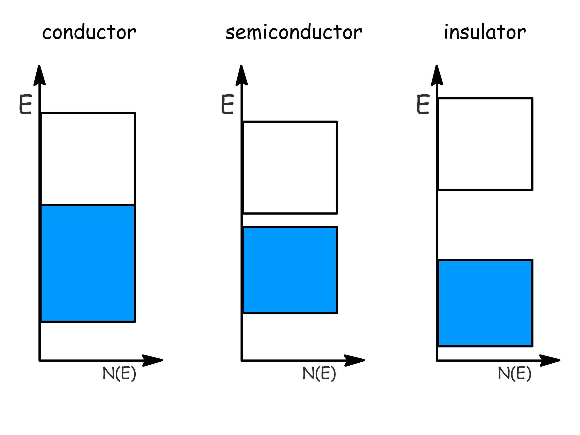
Electrical conductivity arises from partially filled band
- This is bcause electrons can move into unoccupied levels under influence of electric field, which results in net motion of charge
- This allows us to categorize solids into three different types based on their band structures
One way to differentiate conductors from semiconductors is to examine how their conductivity change with temperature
- Conductor's conductivity decrease with increasing temperature as thermal vibrations (phonons) leads to increase in scattering from ion cores and reduces electron mobility
- Semiconductor's conductivity increases exponentially with temperature due to promotion of electrons into empty band
Optical Properties
- Photons of longer than the bandgap pass through the solid, cannot excite electrons into CB
Threshold for absoprtion is a method of determining .
- Note: .
There are two typed of band gaps with regards to optical excitation
- Direct band gaps emerge when the maximum of the valence band and the minimum of the conduction band have the same value, which causes transition by light absorption and emission to be efficient
- Indirect band gaps emerge when the maximum of the valence band and the minimum of the conduction band have the different value, so an optical transition requries change in momentum / , generating a phonon. This makes light absorption / emission inefficient
Mechanism
Conduction within semiconductors happens either via positive charge carrier or negative charge carrier, or both
- The negative charge carriers are the electrons, while the positive charge carriers are the vacant sites ( holes )
- Total current is sum of electron and hole currents
- Moreover, the conductivity is given by
Effective Mass
Electrons in solids behave as though they have a different mass to that of a free electron
- We therefore define an effective mass for both electrons ( ) and holes ( )
- Effective masses of metals are similar to free electron mass but are very different for semiconductors
Effective mass has a huge implication on the energy levels , which in turns affects the density of states
- Larger results in less curved , which means the energy goes up more slowly as k increases
- Since , the density of states decreases with increasing
- Specifically, the size of and affects the conduction band and valence band respectively
Electron Motions
Drift motion of electrons due to an electric field can be described with Drude model
- We can express as
- is the average time between scattering
- and mobility increase with lower effective mass
Random motion due to thermal energy can be modelled using the kinetic theory of gases
- Rearranging it gives us the expression for
Types of semiconductors
There are two types of semiconductors, intrinsic and extrinsic
- The intrinsic semiconductor serves as the quintessential prototype in semiconductor physics, encapsulating all the essential characteristics inherent to this class of materials
- In contrast, extrinsic semiconductors can be envisioned as augmented versions of intrinsic semiconductors. They share the core attributes of intrinsic semiconductors but come with additional elements
¶ Intrinsic Semiconductor
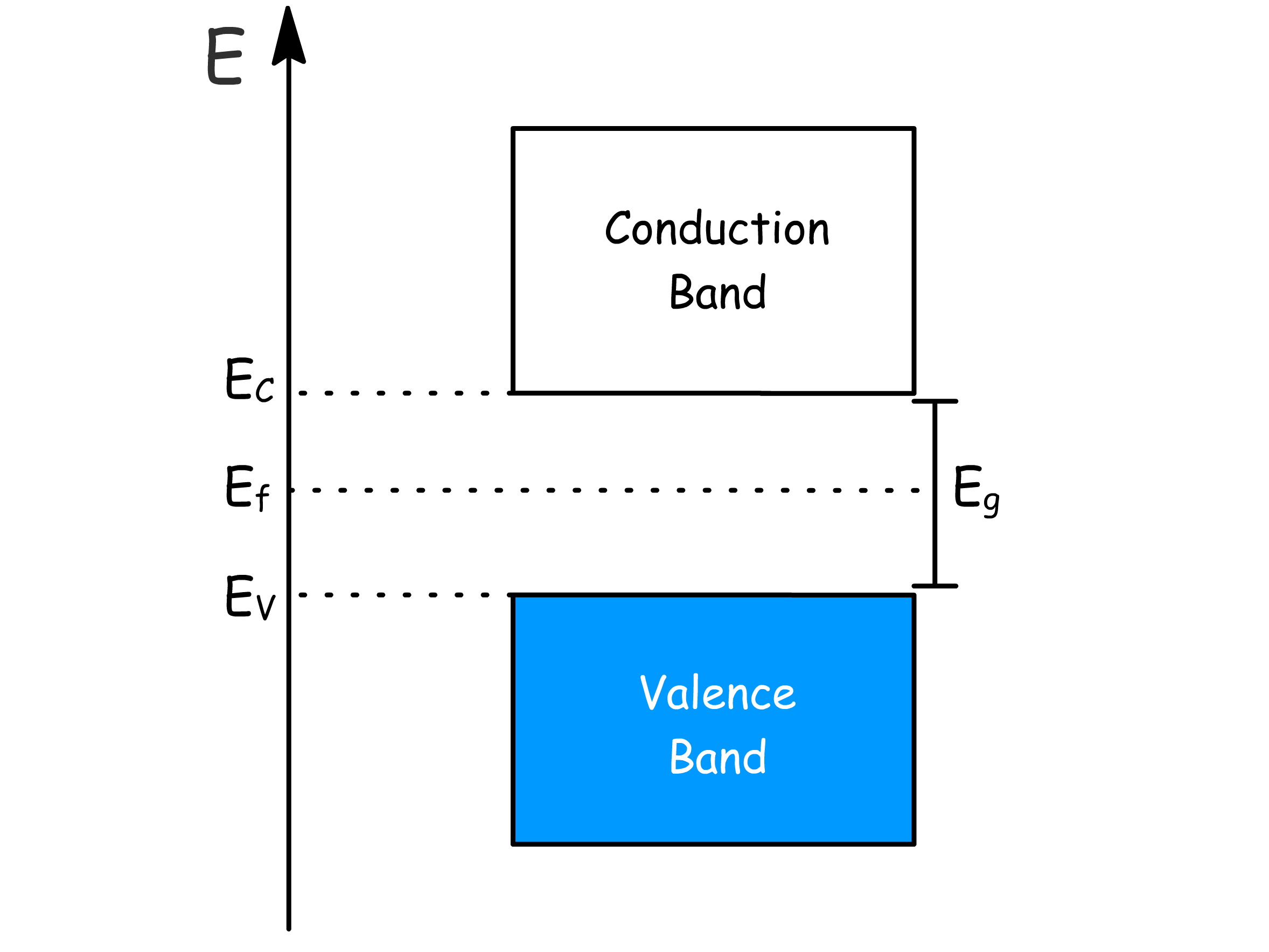
The properties of semiconductors are characterized by two bands
- By convention, we define , which gives rise to the relations
- at or when
- In general at modest temperatures
Carrier Concentration
The positive and negative charge carrier concentration are defined as
- and are the density of states in the conduction and valence band respectively
- and are the probabilities that a state is occupied or unoccupied
- Since the band gap in semiconductor is large such that and , we can approximate the probabilities to
- Putting it all together, the expression for the concentration of ion carriers are given by
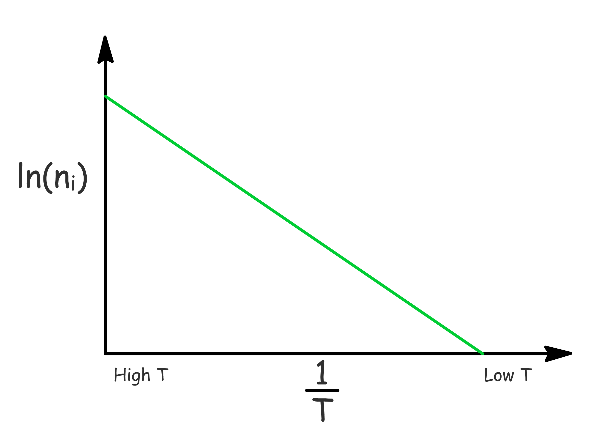
The charge carrier concentration increases with temperature
- One may think that simply by converting the previous expressions to logarithmic form will allow us to plot a straight line graph of or against \frac{1}
- However, the slope in both cases depend on , which is a function of , which will in turn make the plot non-linear
- To get around with this, we simply have to acknowledge that in intrinsic semiconductors and perform some algebaric manipulation
- When we plot it out now, the graph will be essentially linear since the exponential term dominates over
¶ Extrinsic Semiconductor
Intrinsic carrier concentrations in semiconductors are too low to yield the current densities required for most practical applications
- Orders of magnitude increases in concentration can be obtained by doping with electrically active impurities ( doping )
There are two types of doping
- n-type doping and p-type doping
n-type doping
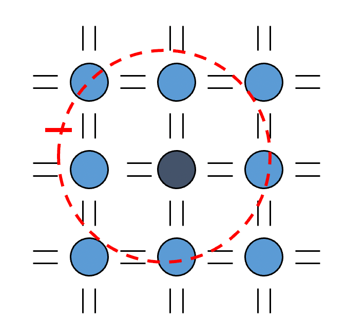
n-type doping happens by fitting an impurity atom which has one more valence electron than the host atoms to fit in the lattice
- The impurity atom should have roughly the same size as the host so that it will fit into the structure without much diffuclty
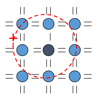
When the impurity atom is electrically neutral, the extra electron is loosely attracted to it
- This is because this electron is not really functioning in a valence bond to hold the crystal together
- Hence, its ionization energy is very small compared to those involved in bonding
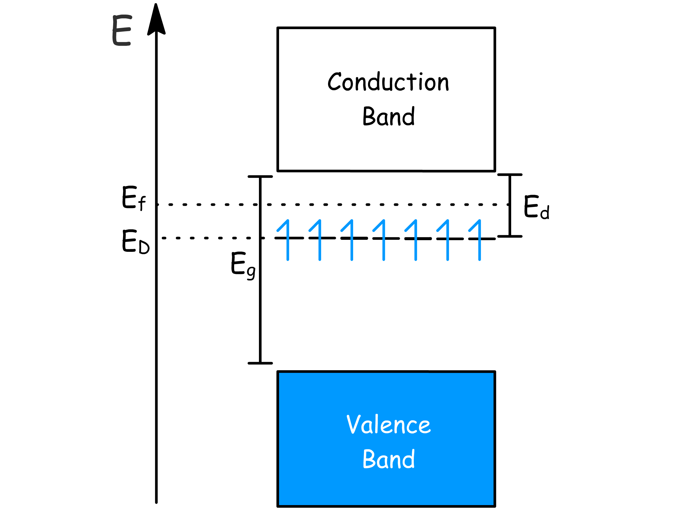
We can easily promote this extra electron to the conduction band
- Upon promoting the electron, the impurity atom will bear a positive charge
- Since the positive ion left behind now has exactly the same number of electrons around it as the host atoms, no hole is formed
- In other words, the charge carriers that arise from this phenomenon are all negatively charged
We can model the behaviour of the electron using the Bohr model with two modifications
- Including a dielectric constant ( )of semiconductor
- We know that the orbits of the electrons must span across a few lattice site since the ionization energy will be comparable to other electrons if it orbits close to the impurity atom
- The effective electric field experienced by the electron from the impurity atom is therefore shielded and a dielectric constant of the medium is needed to account for it
- We use effective mass of electron
- This is because electrons behave as though they have a different mass in solids
Upon making the modification, we will obtain
The introduction of the donor level changes the behaviour of the semiconductor
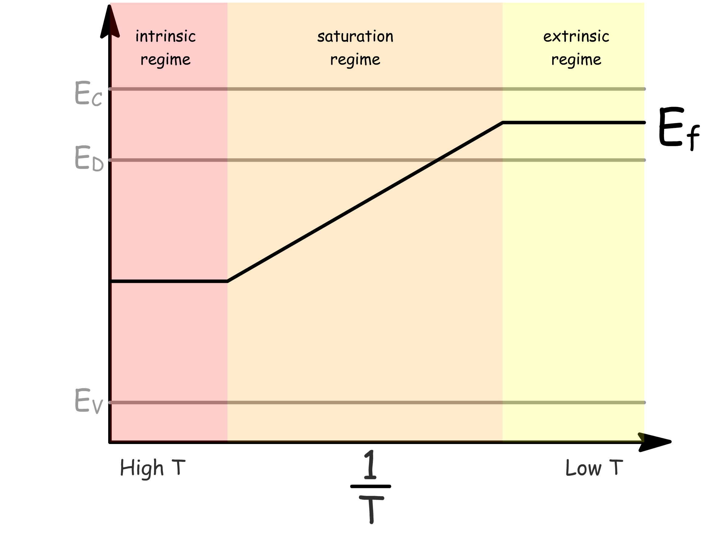
- Increased temperature leads to ionisation of the impurity electrons and thermal excitation into the conduction band, which give rise to conductivity
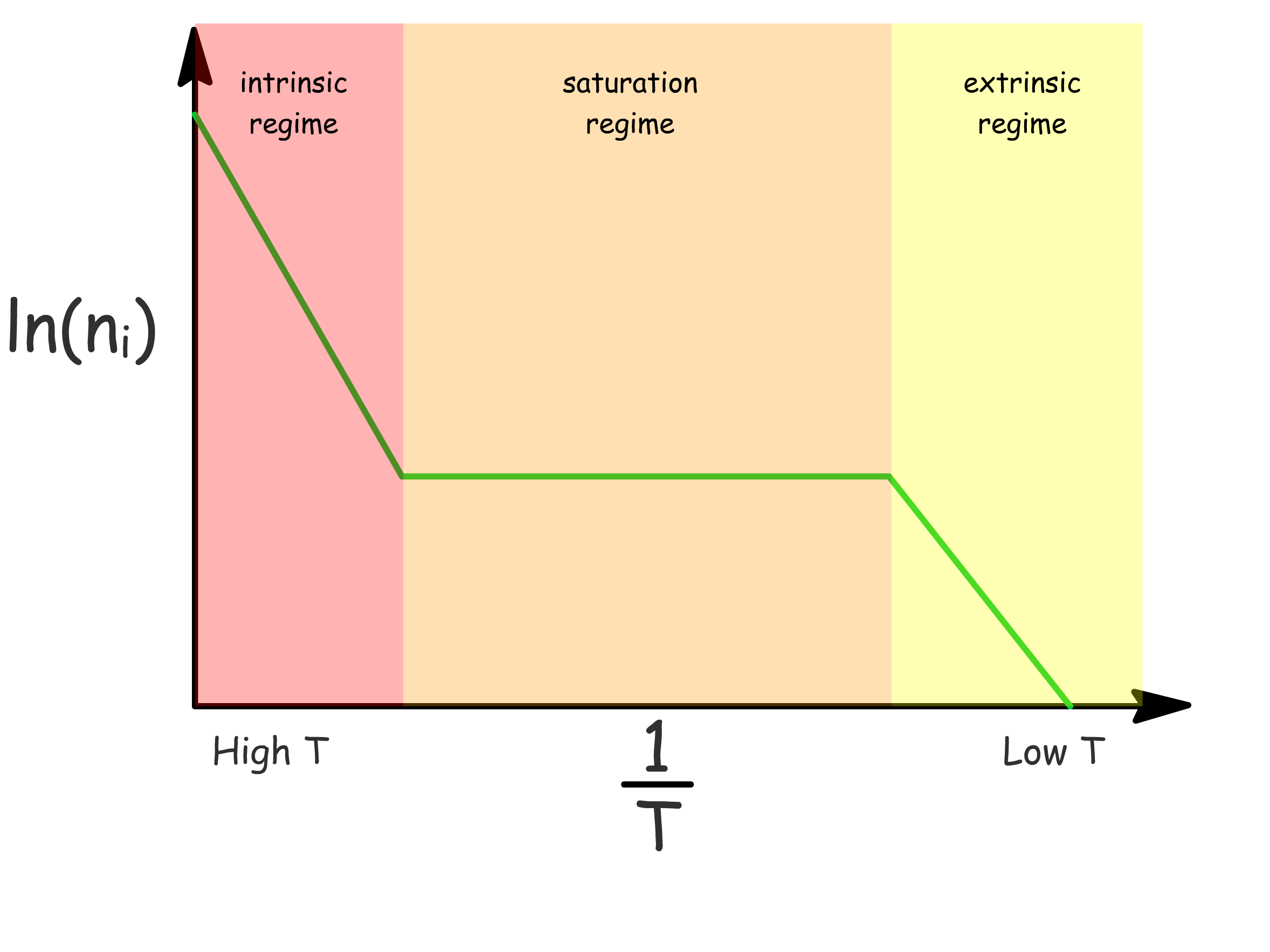
The carrier concentration varys with temperature
- In the extrinsic regime, the increase in carrier concentration is due to thermal excitation from donor levels to conduction band
- In the saturation regime, all donor levels are depleted and remains constant with increasing temperature
- In the intrinsic regime, the increase in carrier concentration is due to thermal excitation from valence band to conduction band
It turns out the Fermi energy also vary drastically with temperature
- In the extrinsic regime, E_f≈E_g-\frac{E_d}
- In the saturation regime, decreases
- In the intrinsic regime,
p-type doping
p-type doping happens by fitting an impurity atom which has one less valence electron than the host atoms to fit in the lattice
- The impurity atom should have roughly the same size as the host so that it will fit into the structure without much diffuclty
When neutal, the impurity atom fails to fill up the bond structure in its neighbourhood
- Since the bonding within the lattice is very strong, completing the bond structure at the cost of a neighboring bond will only cost very little energy
We can easily promote this electrons from the valence band to the acceptor level
- Upon promoting the electron, the impurity atom will bear a negative charge. But since anion is fixed in place, it cannot carry charges
- In other words, the charge carriers that arise from this phenomenon are all positively charged holes from the valence band
We can model the behaviour of the holes using the Bohr model with two modifications
- Including a dielectric constant ( )of semiconductor
- We know that the orbits of the hole must span across a few lattice site since the energy needed to promote an electron to the acceptor level will be comparable to that needed to the conduction band if it orbits close to the impurity atom
- The effective electric field experienced by the hole from the impurity atom is therefore shielded and a dielectric constant of the medium is needed to account for it
- We use effective mass of hole
- This is because holes behave as though they have a different mass in solids
Upon making the modification, we will obtain
- the ionization energy of the hole can be regarded as the energy needed to remove it by promoting an electron to fill it up
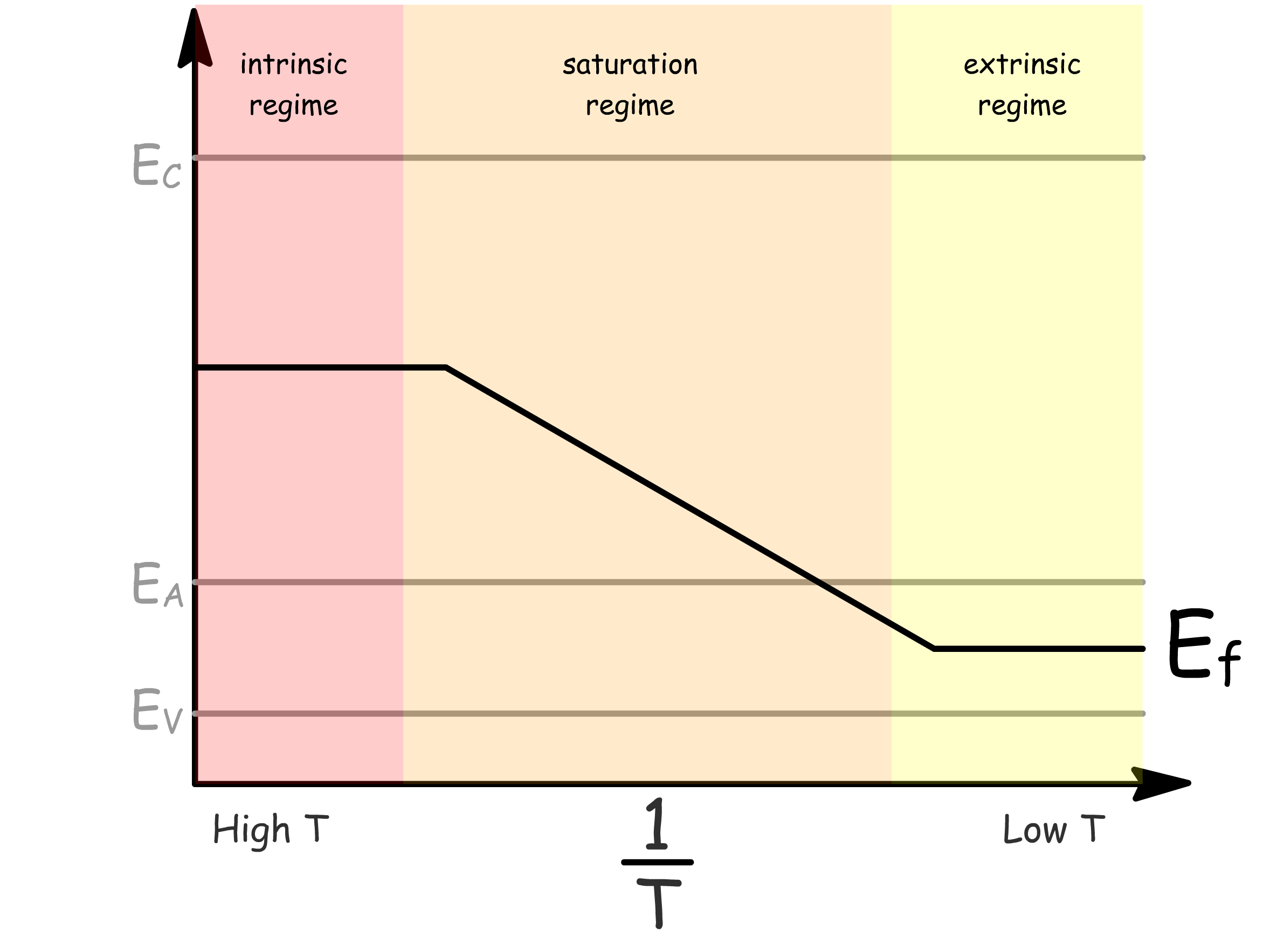
The introduction of the acceptor level changes the behaviour of the semiconductor
- Increased temperature leads to promotion of the valence band electrons to the acceptor level, which give rise to conductivity
The carrier concentration varys with temperature
- In the extrinsic regime, the increase in carrier concentration is due to thermal excitation from valence band to acceptor levels
- In the saturation regime, all acceptor levels are full and remains constant with increasing temperature
- In the intrinsic regime, the increase in carrier concentration is due to thermal excitation from valence band to conduction band
It turns out the Fermi energy also vary drastically with temperature
- In the extrinsic regime, E_f≈\frac{E_g}
- In the saturation regime, increases
- In the intrinsic regime,
p-n Junction
The free energy of the conduction band electrons depends on their concentration
- Upon some algebaric manipulation, we will obtain
- We can then compare it to the expression of chemical potential in solution
- The free energy of electrons in the conduction band is given not by but by
- Electrical voltage is determined by difference in not band energies
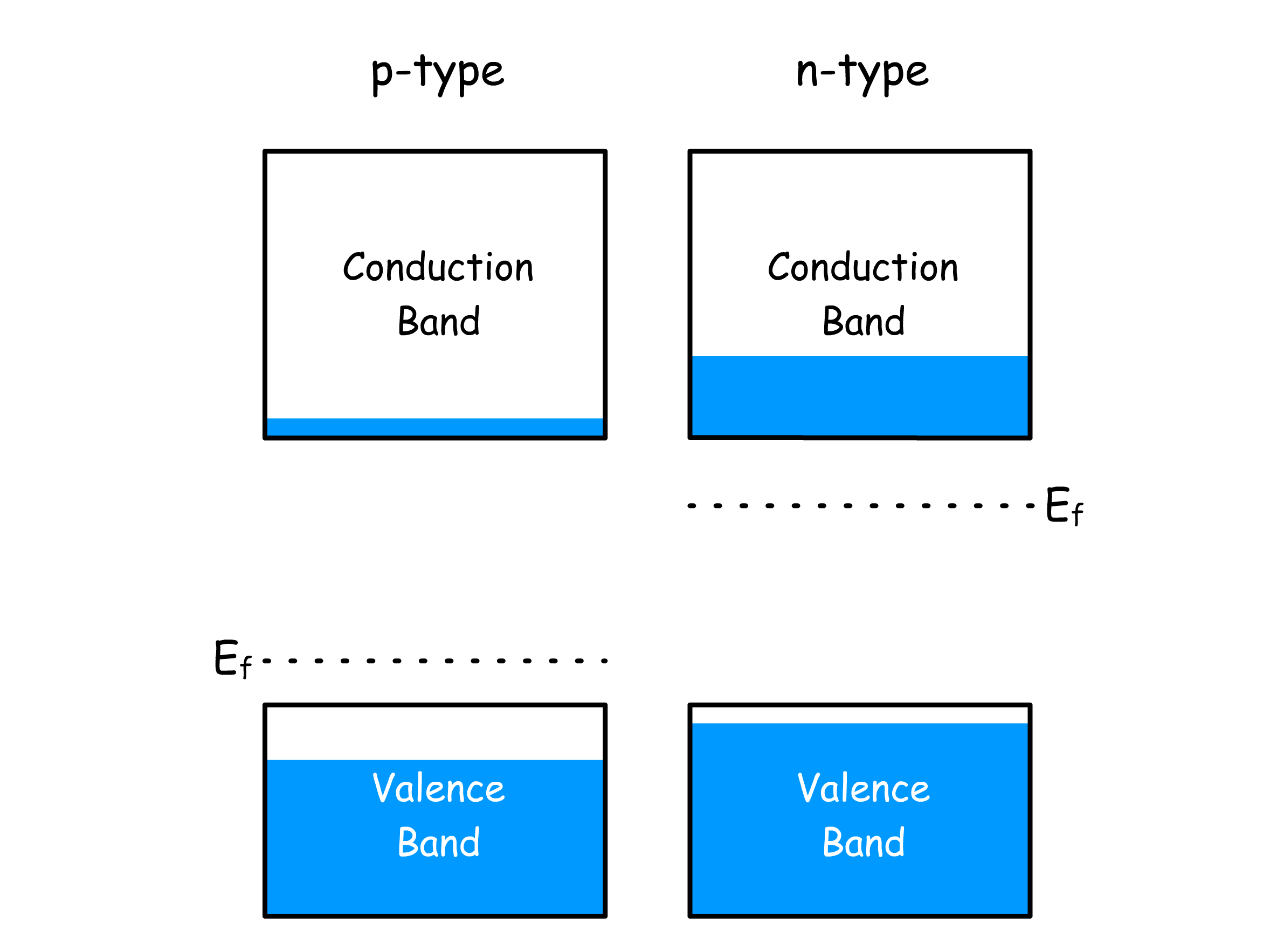
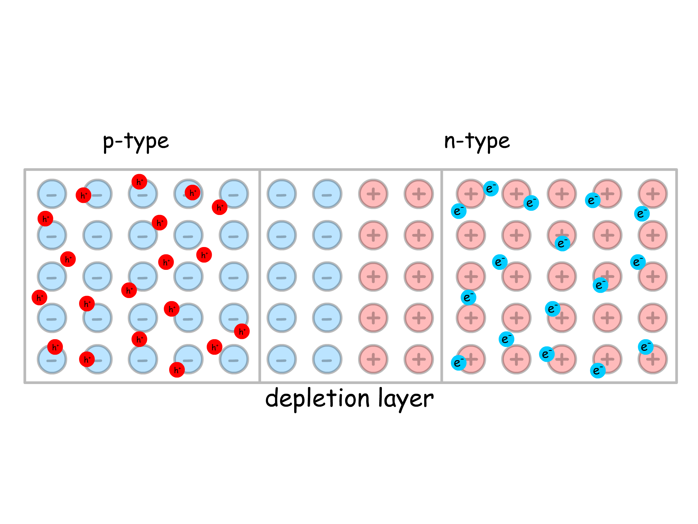
An interesting phenomenon arise when we connect a p-type semidconuctor to an n-type semiconductor
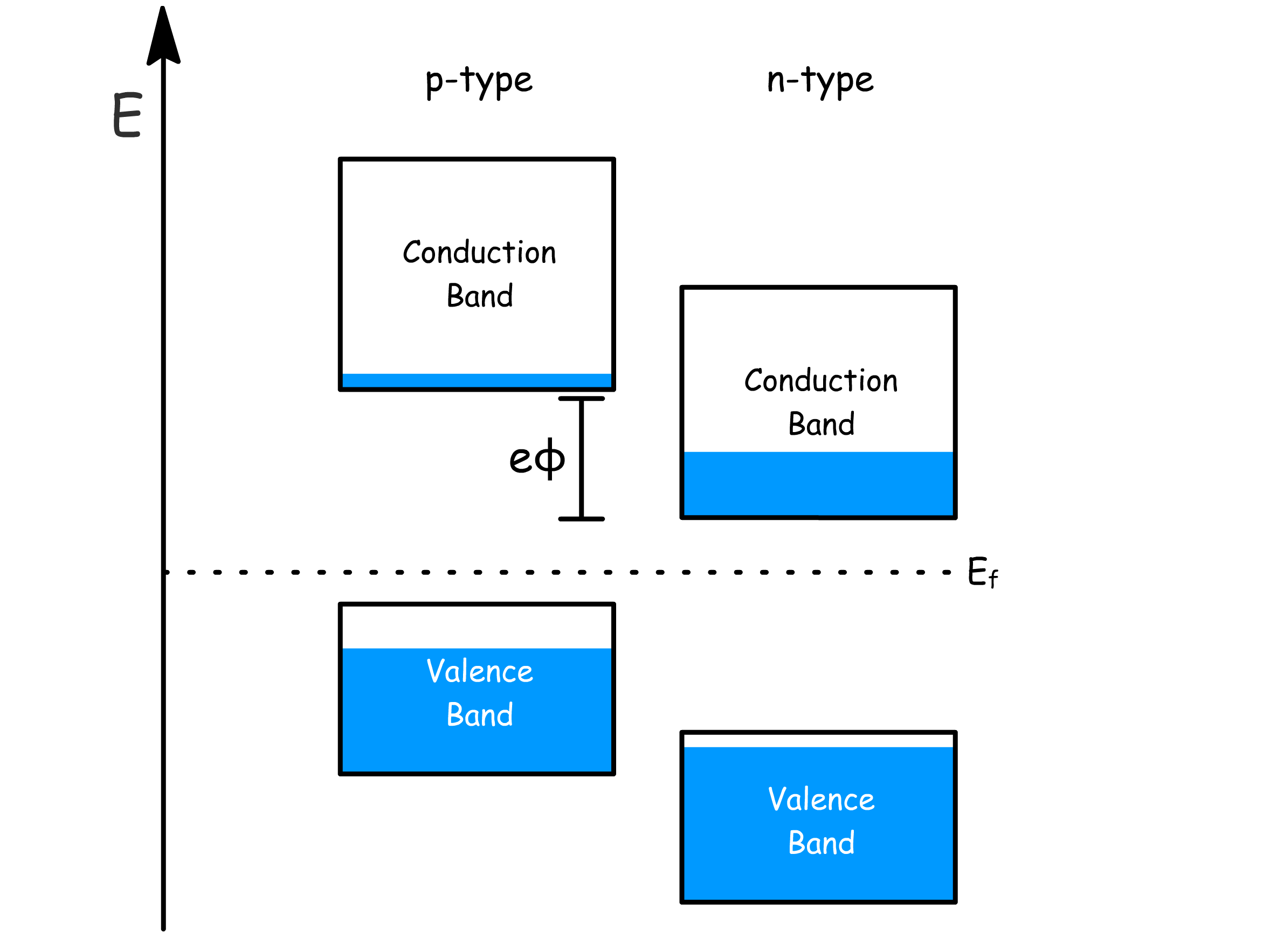
- When they are separated, they have different Fermi energy because they clearly have different concentration of conduction band electrons
- Upon contact, the diffusion of carriers in the junction eliminates the holes and conufction electrons in that region, leading to a depletion layer with virtually no carriers
- Within the depletion layer, the ions are properly ionized, resulting in a contact potential ( )
- Since Fermi energy is the same as free energy, they are aligned at equilibrium
Depending on the external voltage applied, the electronic motion, and hence the current, will differ greatly
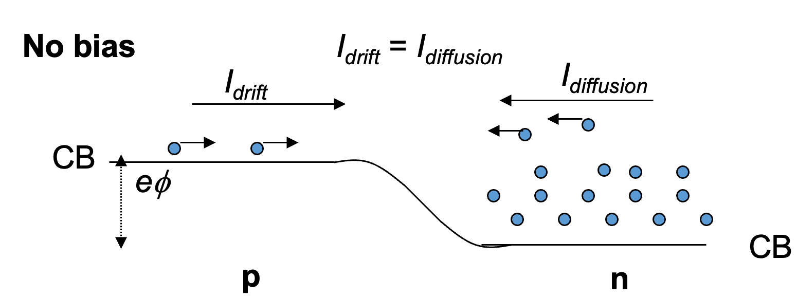
1. No bias ( equilibrium )
- is the current due to electrons (with sufficient energy) diffusing from n to p region
- is the current due to electrons diffusing from p to n region due to built in electric field in junction
2. Forward bias ( n-side made negative )
- Voltage difference is reduced ( )
- More electrons diffuse from n to p region with net flow of electrons
3. Backward bias ( n-side made positive )
- Voltage difference is increased ( )
- Less electrons diffuse from n to p region with net flow of electrons
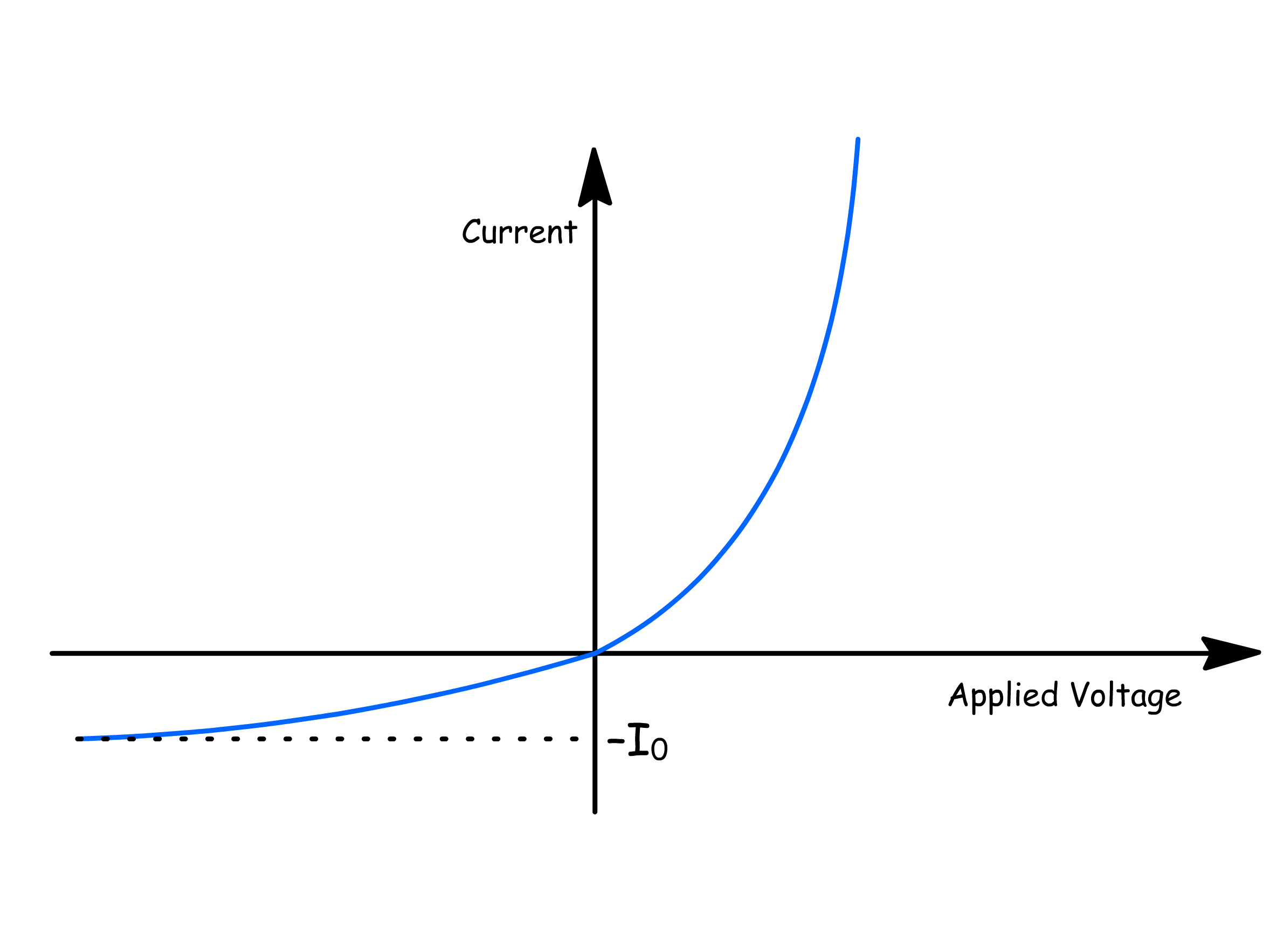
We are now in a position to plot out how the current changes with applied voltage
- The current in the forward bias domain is given by
- The current in the backward bias domain is given by
