¶ Solution-Processed Electronic Materials
Inorganic semiconductors such as silicon (Si), gallium arsenide (GaAs), indium phosphide (InP), and gallium phosphide (GaP) have dominated the electronics industry for the past 40 years.
Pros:
- Highly controlled structure, allowing for precision in design and functionality.
- High-performance materials with excellent conductivity and optical properties.
Cons:
- Manufacturing challenges, including the need for ultra-clean environments.
- Expensive, especially as device sizes increase.
- Limited to small-area devices due to batch processing techniques.
Solution-processed materials introduce new possibilities for semiconductor production using cost-effective and scalable techniques, such as blade coating, spin coating, and screen printing, similar to how newspapers are printed.
- Large-scale Production: These materials make it feasible to create thin-film semiconductors for large surfaces. For example, a photoactive layer can be coated over a broad area.
- Cost-Efficient: Fabrication is considerably cheaper, with costs ranging from a few hundred to a few thousand pounds, far less than inorganic semiconductors.
¶ Organic Semiconductors
Organic semiconductors offer flexibility and a promising future for low-cost, lightweight electronic devices.
- Flexible Design: Their organic nature makes them inherently flexible, ideal for applications in wearable technologies and flexible electronics.
- Improved Efficiency: Organic solar cells have shown significant progress, with efficiency rates now approaching 20%, almost comparable to traditional silicon and perovskite-based solar cells.
- Large-scale Viability: Massive manufacturing setups, such as the large screen printer in Finland, demonstrate the potential for industrial-scale production.
Owing to its unique properties, there are a lot of new applications:
- Organic field-effect transistors (OFETs): Essential for biological sensors due to their biocompatibility with brain tissue.
- Biological and chemical sensors
- Organic lasers: A potential breakthrough area for organics.
- Batteries
- Long-term Goal: The ultimate aim is to develop fully plastic electronic technologies that incorporate various components fabricated using solution processing.
¶ Perovskites
Perovskites are an exciting class of materials that share a crystal structure similar to the mineral perovskite (calcium titanoate, ). These materials have the general formula , where:
Advantages of using perovskites
- Space Applications: Due to their high power-to-weight ratio, perovskites are ideal for space exploration, unlike heavier silicon. They also remain stable under gamma radiation.
- Optoelectronic Properties: Unlike organic semiconductors, perovskites have direct band gaps (), giving them a high extinction coefficient, allowing them to be processed into thin films while maintaining excellent light absorption and emission characteristics.
- High Carrier Mobility: Their crystalline structure supports superior charge carrier mobility, making them highly efficient.
- Tuning Properties: By adjusting the composition of A, B, and X sites in the perovskite formula, the band gap and other electronic properties can be customized. The s and p orbitals of the B²⁺ and the p orbitals of X⁻ contribute to the frontier orbitals, making perovskites highly tunable.
- Complementarity with Silicon: Unlike organic semiconductors, perovskites can complement silicon-based technologies, such as in tandem solar cells. Oxford PV, led by Professor Harry Snaith, has recently commercialized silicon-perovskite solar cells.
- X-ray Detectors: Perovskites excel at absorbing and emitting X-rays, offering higher sensitivity than traditional silicon or selenium-based detectors, which require larger machines to compensate for their inefficiencies.
Perovskites' Defect Tolerance
Defects in perovskites can introduce energy levels within the band gap, trapping charges in them and decreasing conductivity:
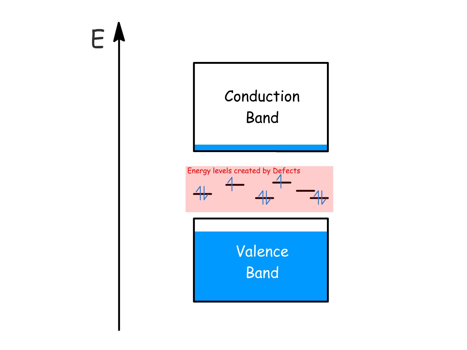
There are two main types of energy levels that are caused by defects
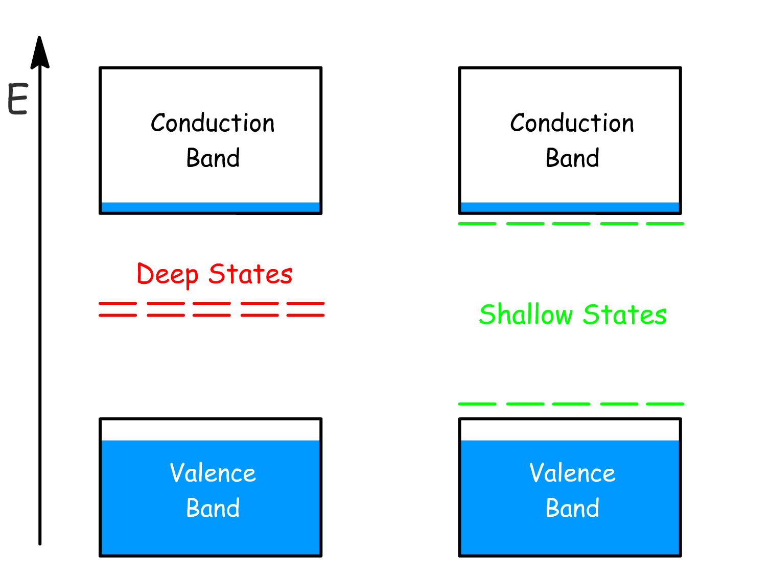
- Deep states: Located near the middle of the band gap, these traps result in current loss.
- Shallow states: Found near the band edges, these defects allow charges to escape back into the conduction and valence bands through thermal detrapping.
Defects in perovskites mostly introduce shallow states
- Unlike other materials that require precision, perovskites tolerate defects well, which allows for more flexibility in fabrication.
¶ Excitation of States
¶ Polarons
Organic semiconductors are excitonic materials, meaning that they need to support and sustain excitation
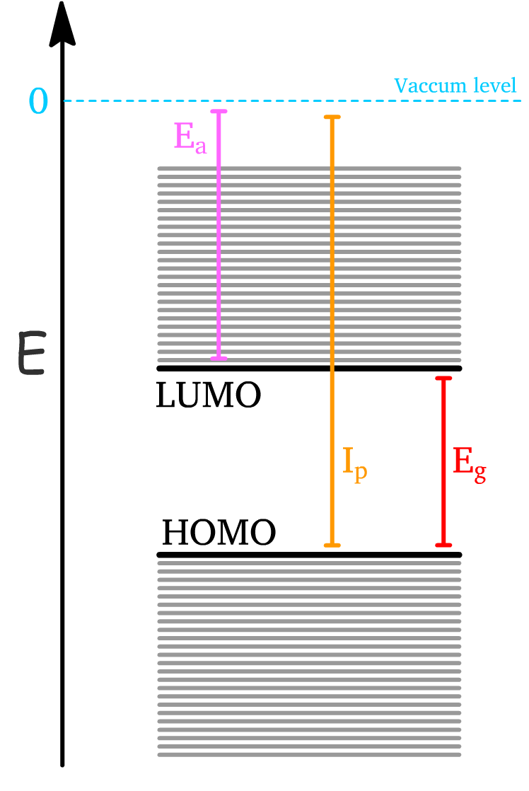
- Electron Affinity () is the energy gained by injecting an electron to the LUMO from the vaccum level
- Ionization Potential () is the energy required to excite an electron from HOMO to the vaccum level
- The band gap energy () is the energy required to excite an electron from HOMO to the LUMO
When electron is taken away from the HOMO or injected to the LUMO, this results in the formation of radical ions
- These radical ions are termed electron polaron and hole polaron
The presence of charges will disrupt to molecular or lattice structure
- When these charges move through a material, it distorts the structure via the electrostatic forces. This distortion creates a local deformation or "cloud" of lattice vibrations (phonons) around the electron.
- In essence, a polaron is a charge carrier that moves through a material, accompanied by this cloud of lattice distortion.
Polarons can result in the formation of new energy levels within the band gap of the material
- This is because the lattice vibrations (phonons) is interacting with the electronic states and the change in molecular configuration around charge reduces the energy of the system

- Since the charge is somewhat trapped by its interaction with the surrounding lattice, the resulting polaron can occupy energy states that differ from those of a free electron or hole. This "self-trapping" creates energy levels within the band gap.
¶ Exciton
Exciton is a bound state of an electron and a hole in an insulator or semiconductor.
- Since the positive and negative polarons are bound together by the Coulomb force, exciton as an entity does not have a net charge
We can understand the concept of exciton using different perspective
- Under the band-picture, an exciton consists of an electron in the conduction band bound to a hole in the valence band.
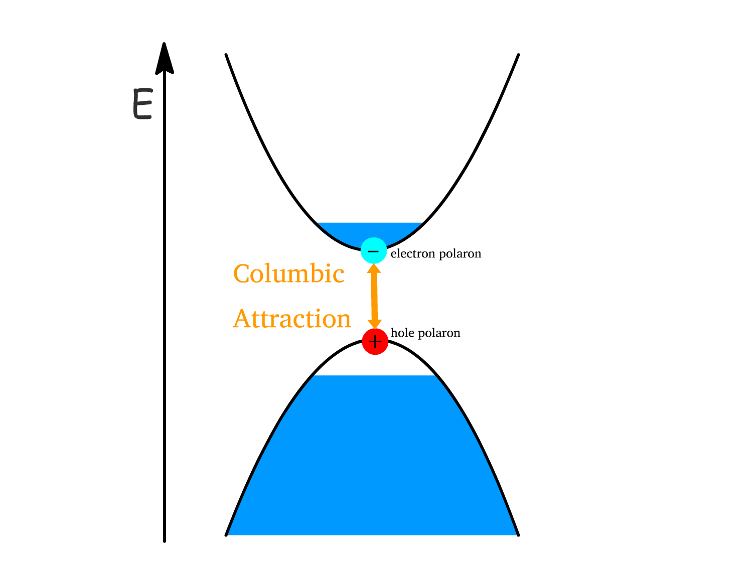
- For a molecular picture, it consists of an electron in an unoccupied, high energy orbital and a hole in an occupied, low energy orbital
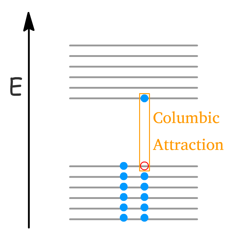
- If we look at the lattice or molecular structure, an exciton is just the electron-hole pair moving together as a unity
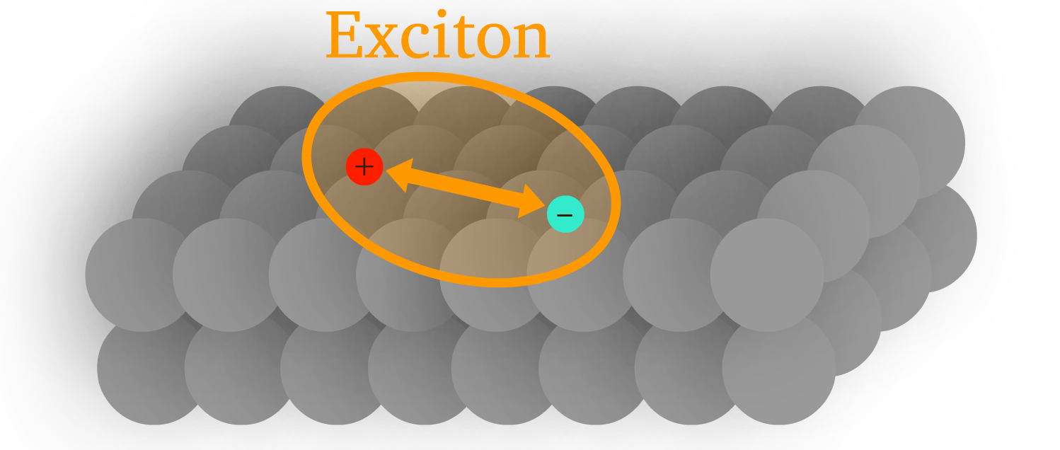
The energy of an exciton is lower than the sum of the individual energies of the electron and hole.
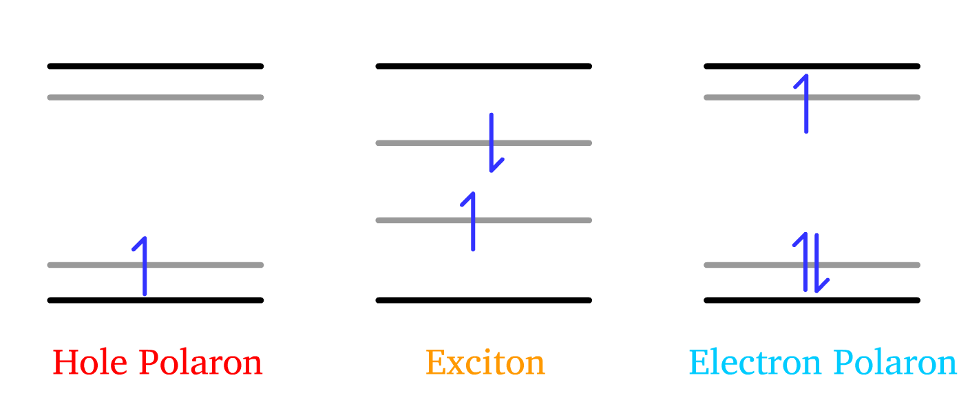
- This energy reduction is due to the Coulombic binding energy between the two polarons.
The exciton binding energy () is defined as the energy required to separate the electron and hole into free charges
- Coulomb interaction between two-point charges is screened by the dielectric constant .
There are two types of excitons that arise due to the variation in dielectric constants.
- Wannier-Mott Exciton ( Typically in Inorganic Semiconductors )
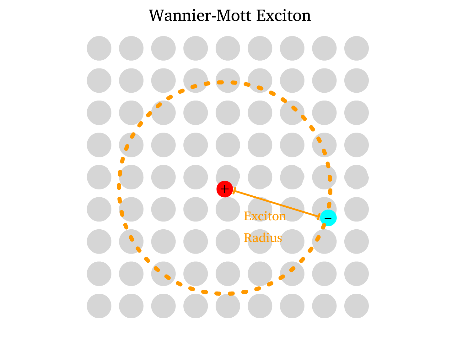
- The lattice of ions in inorganic semiconductors provides significant screening for the Coulombic interaction, thus resulting in High Dielectric Constant
- Due to the weak Coulombic binding, the electron and hole can be far apart in the crystal lattice, resulting in a large exciton radius and low binding energy.
- Frenckel Exciton ( Typically in Organic Semiconductors )
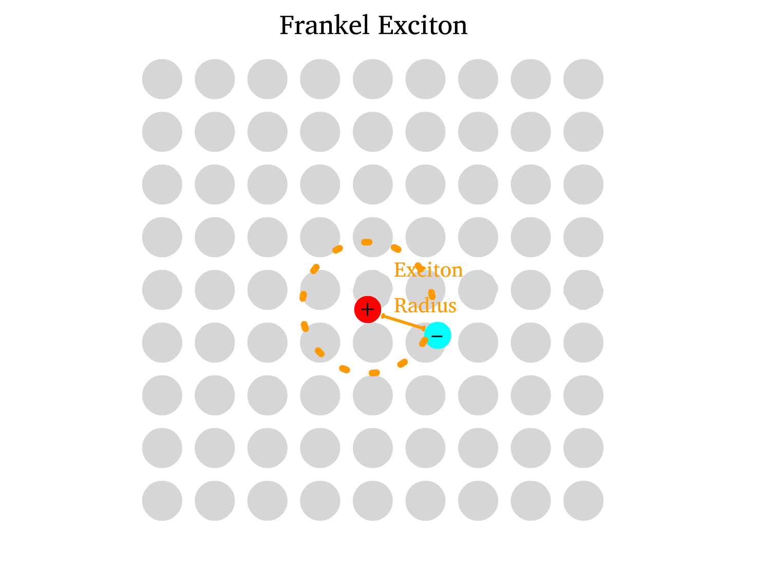
- The absence of crystalline structure results in weak screening for the Coulombic interaction, thus resulting in Low Dielectric Constant
- Due to the strong Coulombic binding, the electron and hole are close together, resulting in a large exciton radius and high binding energy.
The order of magnitude of the binding energy is important
- When , electron and hole will be easily dissociated
- When , electron and hole will be stable to dissociation
¶ Exciton Lifetime and Diffusion
When an exciton decays, the electron and hole recombine, releasing energy in the form of light or heat.
- This recombination process mirrors those in photochemistry, involving internal conversion (IC), intersystem crossing (ISC), fluorescence, and phosphorescence.
- OLEDs (Organic Light Emitting Diodes) leverage both fluorescence (short-lived) and phosphorescence (long-lived, radiative emission) to achieve high external quantum efficiency (EQE) and brightness in displays.
The quantum efficiency () of exciton emission refers to the fraction of absorbed photons that are re-emitted as light, whether through fluorescence or phosphorescence:
- The quantum efficiency is directly proportional to the exciton lifetime, which determines how long the exciton exists before recombination occurs.
- These lifetimes can be experimentally determined using techniques like Time-Correlated Single Photon Counting (TCSPC) and Transient Photoluminescence
Exciton Diffusion
The Frank-Condon Principle predicts that emission and absorption spectra should be mirror images. However, in practice, exciton diffusion results in red-shifted emission due to energy loss during diffusion.
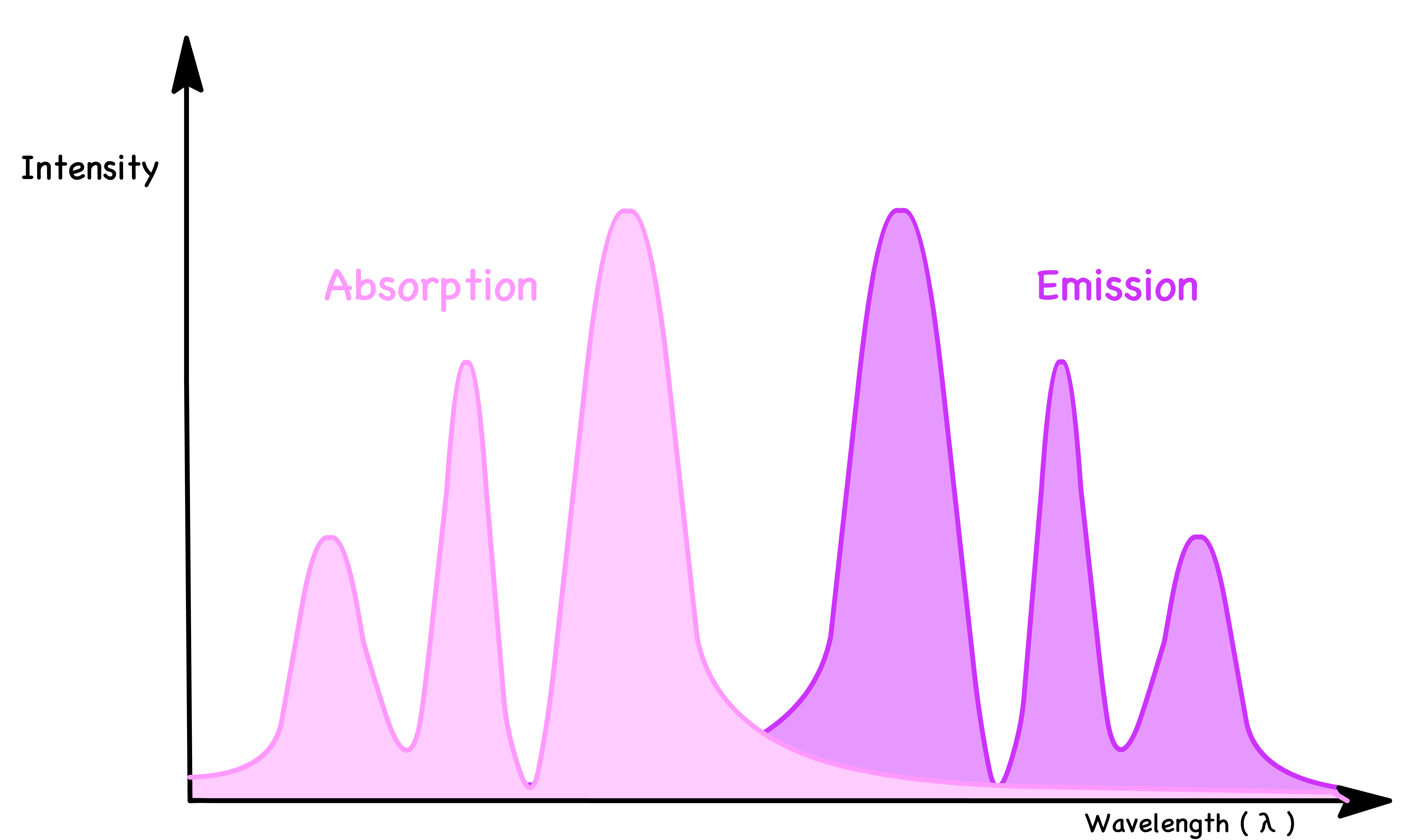
Exciton diffusion refers to the movement of excitons from higher energy states (larger band gaps) to lower energy states (smaller band gaps)
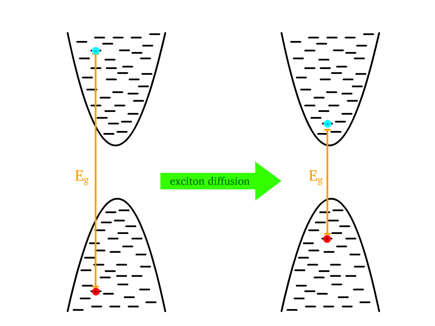
- This occurs because excitons naturally relax to lower energy regions, especially in organic semiconductors with long chains of varying structure and packing, creating regions with different energy levels and band gaps.
- Due to exciton diffusion, the molecule that absorbs light is often not the one that emits light. The exciton can migrate before recombination, leading to different emission sites within the material.
The exciton diffusion length is the average distance an exciton travels before recombining.
- In organic materials, this distance is typically short (2-10 nm) due to strong localization of excitons.
- Improving molecular packing or introducing energy gradients can enhance exciton diffusion and improve device efficiency.
Exciton diffusion is essential in organic devices like solar cells, OLEDs, and organic lasers
- In organic photovoltaics, excitons must diffuse to the donor-acceptor interface for charge separation. If excitons recombine before reaching this interface, energy is lost as heat, reducing efficiency.
- In OLEDs, efficient exciton diffusion allows for effective light emission by transferring energy to emissive regions.
Dopant
Dopants can be introduced to polymer LEDs to adjust the emitted color.
- The polymer is primarily used for charge transport, while the dopant controls the color of the emission.
As the concentration of dopant molecules increases, the emission shifts from being predominantly from the polymer host to predominantly from the dopant (guest) molecules.
- The mechanism for this energy transfer is the Förster Transfer Mechanism, where energy is non-radiatively transferred from the host polymer to the dopant.
Dopant data can be utilized to estimate the diffusion range of excitons in a polymer film.
- To estimate the number of dopant molecules per unit volume in the polymer, we use
¶ OLED and Photovoltaics
OLEDs (Organic Light Emitting Diodes) and photovoltaics operate on opposite principles, yet the physical mechanisms that govern their operation are highly complementary.
- A good OLED can theoretically be repurposed to function as a solar cell by reversing the processes, highlighting their shared dependence on charge injection, transport, and recombination.
In OLED and photovoltaics, two electrodes (the cathode and anode) are connected through a semiconductor.
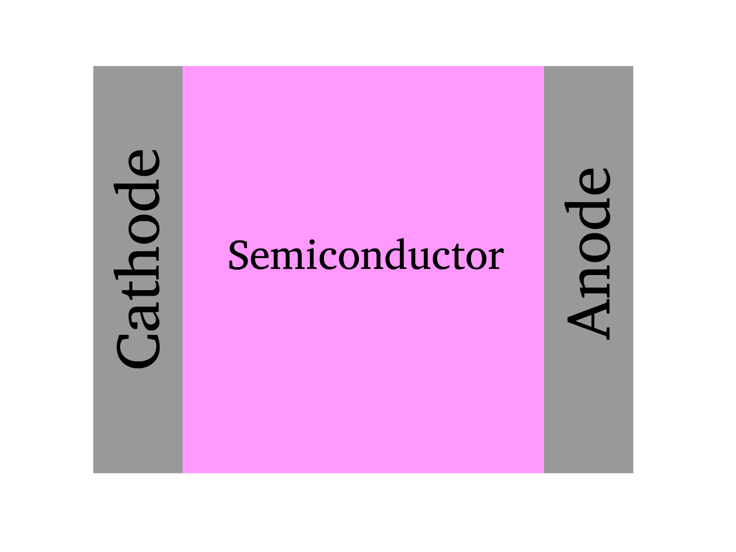
The properties of these electrodes are determined by their workfunction.
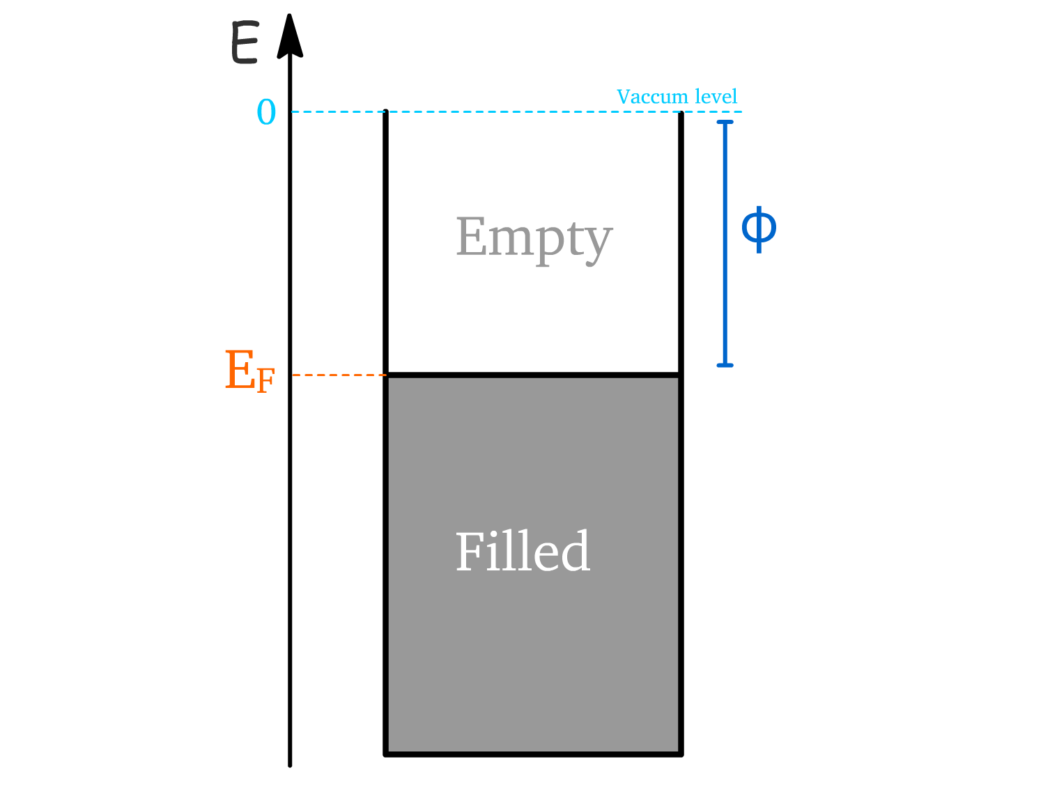
- The workfunction () is the energy required to remove an electron from a material and move it to a point just outside the surface (into a vacuum).
- It is defined as the energy difference between the Fermi level () and the vacuum level ().
- The Fermi level represents the highest occupied energy state at absolute zero and is equivalent to the chemical potential of the material.
The classification of an electrode as a cathode or anode depends on the relative size of their workfunctions
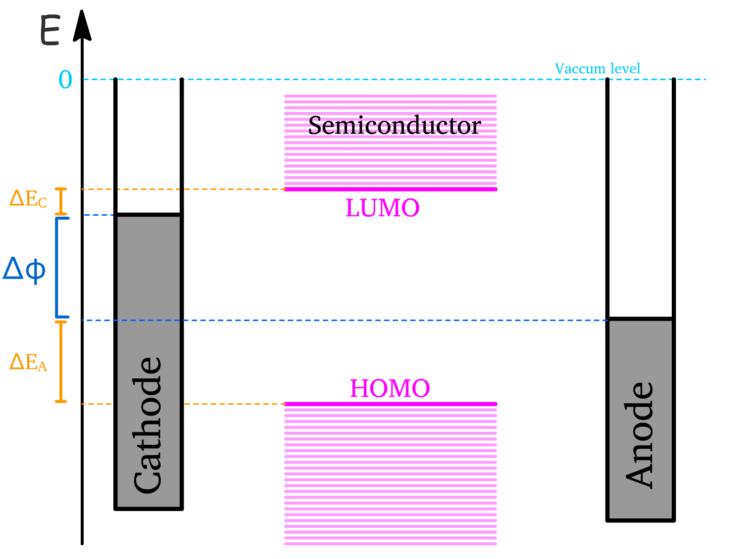
- The electrode with the lower workfunction becomes the cathode (injects electrons).
- The electrode with the higher workfunction is the anode (injects holes).
When the electrodes are connected through the semiconductor, the system seeks equilibrium by aligning the Fermi levels of the two electrodes.
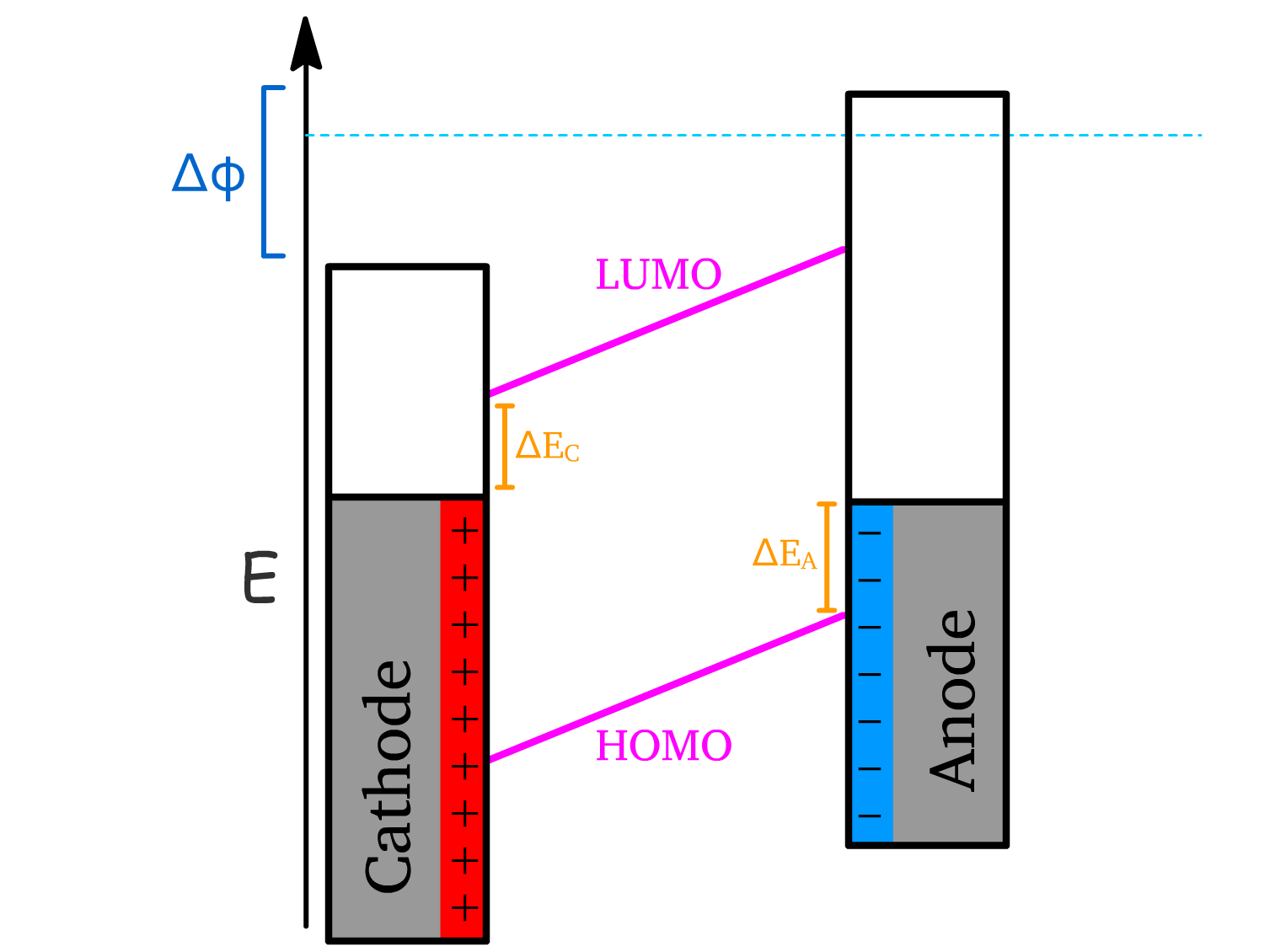
- This is achieved by the movement of electrons from the cathode to the anode through the semiconductor.
- This migration of charge causes a charge buildup at both electrodes and results in a slanting of the semiconductor’s energy levels.
¶ OLED
In an OLED, an external voltage is applied to drive the generation and recombination of charges, ultimately producing light via electroluminescence.
Operation Principle
1. Apply Forward Bias
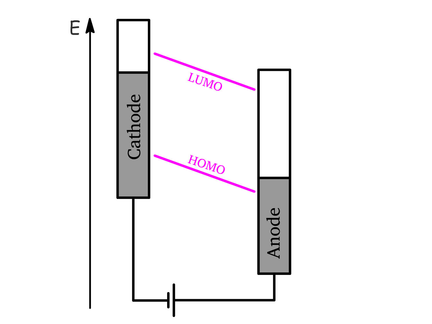
- A voltage is applied to overcome the difference in workfunctions between the anode and cathode.
- The large forward bias** () causes the energy levels of the semiconductor to slant in the direction that facilitates charge injection.
2. Charge Injection:
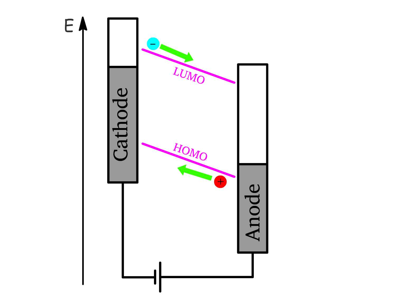
- Hole injection: Holes are injected into the semiconductor from the anode, which corresponds to the oxidation of molecules at the interface.
- Electron injection: Electrons are injected from the cathode, corresponding to the reduction of molecules at the cathode interface.
3. Charge Transport:
- Polarons are transported through the semiconductor by hopping, facilitated by the applied electric field.
- Electrons and holes hop from one molecule to another via "reduction-oxidation" reaction () and "oxidation-reduction" reaction (). respectively
4. Exciton Formation:
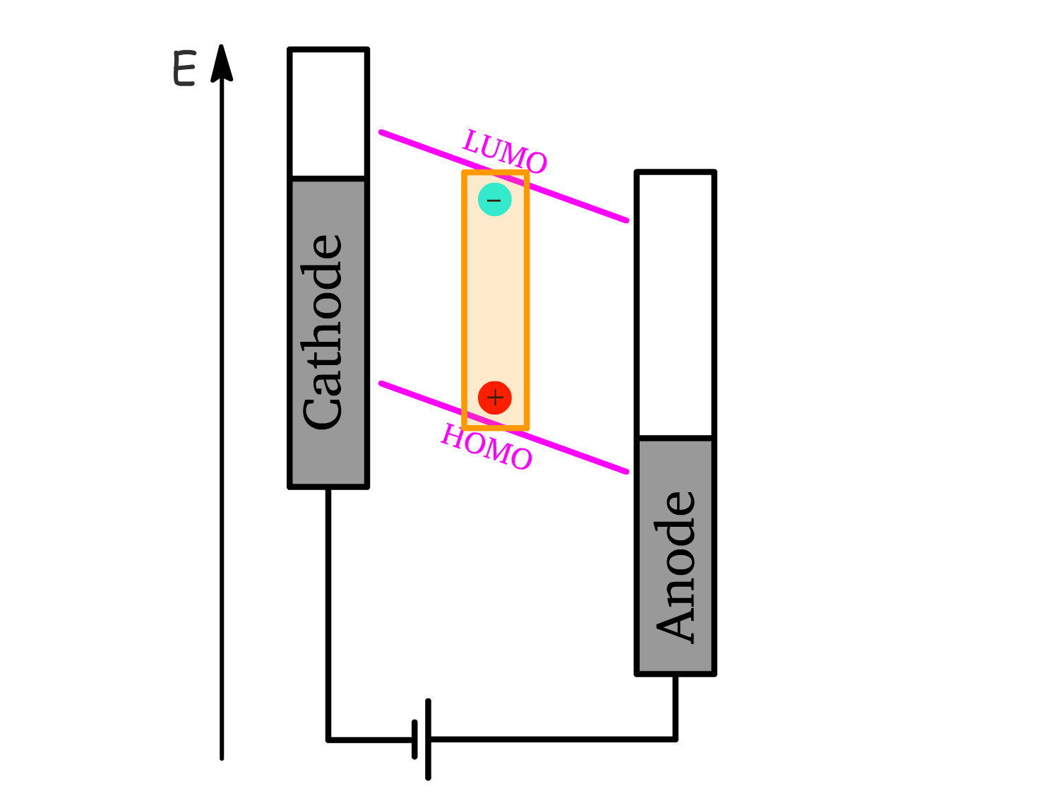
- Once hole and electron polarons meet within the active layer, they form an exciton.
5. Exciton Recombination (Electroluminescence):
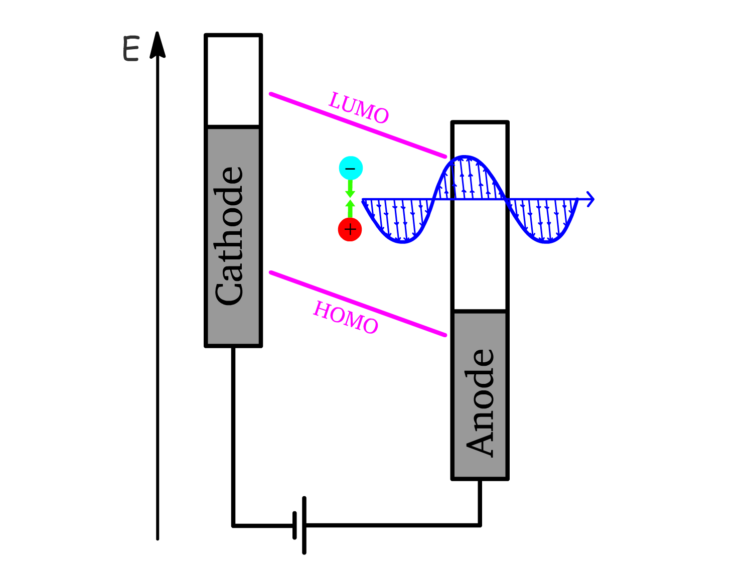
- The exciton undergoes radiative decay, recombining and releasing its energy as light.
- This process is called electroluminescence, which is the primary light-emission mechanism in OLEDs.
Charge Injection Mechanisms under Strong Forward Bias
In Step 1, we emphasized that a strong forward bias is necessary for efficient operation in OLEDs.
- Thermodynamically, any forward bias () should initiate charge injection
- However, a strong forward bias () is needed to overcome the kinetic barriers and force the energy levels of the semiconductor to slant sufficiently, making charge injection favorable.
Mechanism 1: Thermal Excitation
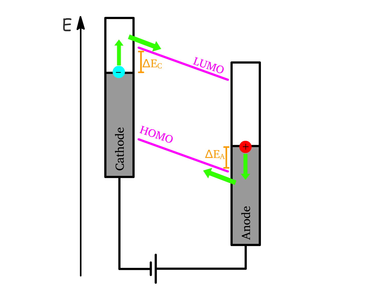
- Electrons (from the cathode) and holes (from the anode) require additional energy to jump from their respective Fermi levels into the conduction band and valence band of the semiconductor.
- The energy gaps ( for electrons, for holes) can be thermally overcome if
Mechanism 2: Quantum Tunneling
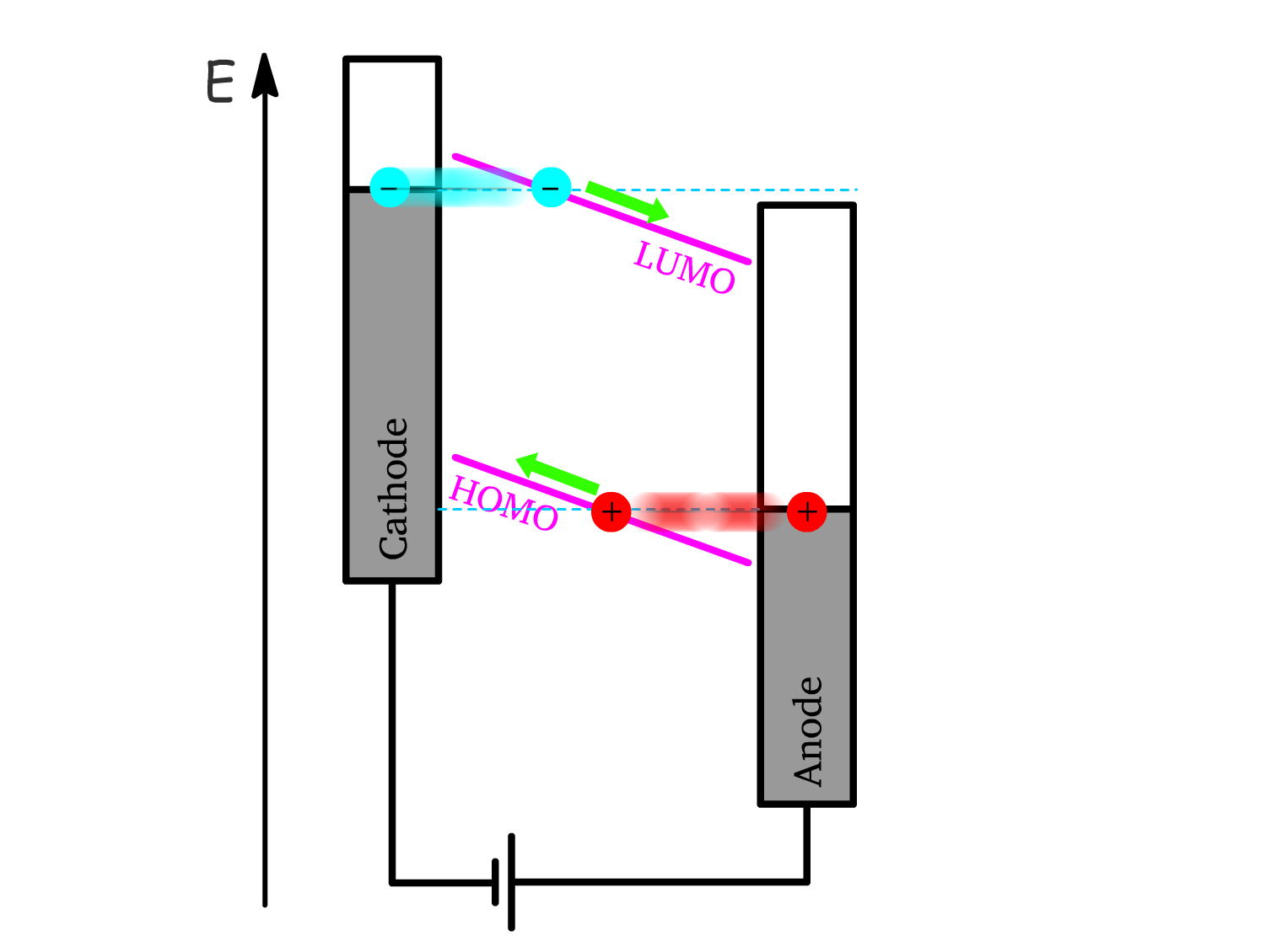
- When part of the conduction band (CB) is below the Fermi level of the cathode, and part of the valence band (VB) is above the Fermi level of the anode, electrons and holes can simply tunnel through the potential barrier formed by the energy offset.
- A strong forward bias lowers this barrier, increasing the likelihood of quantum tunneling, allowing electrons and holes to directly enter the conduction and valence bands
Electroluminescence from an LED
Electrically generated excitons in an LED behave the same as optically generated excitons.
- This means the electroluminescence (EL) spectrum can be controlled and predicted by adjusting the photoluminescence (PL) spectrum of the polymer.
The luminosity of the LED (measured in is proportional to the current density (J):
- To optimize performance, we aim to maximize current density (J) for a given voltage while keeping power consumption minimal. ()
The luminous efficiency (), measured in Candela per Ampere (), quantifies how efficiently the current is converted into light:
- This equation can be used to estimate the efficiency of the OLED at specific drive voltages
Wall-plug efficiency () is the ratio of power out (emitted light) to power in (input electrical energy).
External Quantum Yield
The external quantum yield () represents the efficiency with which excitons lead to radiative decay (light emission) in a device like an OLED.
- Each factor represents a different physical process influencing the overall quantum yield
- Defined as the fraction of current that results in exciton formation
- Represents the ratio between the electron-hole recombination current () and the total current passing through the device ()
- This represents the fraction of excitons that are capable of radiative decay.
- It is determined by the singlet-to-triplet ratio. This ratio governs how many excitons can emit light. In most organic materials, singlet excitons emit light efficiently, while triplet excitons tend to decay non-radiatively.
- If electron and hole spins combine randomly, then , meaning that only 25% of excitons (singlet excitons) can decay radiatively.
- Intrinsic photoluminescence quantum yield: The fraction of excitons that decay radiatively by emitting photons rather than non-radiatively.
- It is a property of the material itself and is given by the ratio of the radiative decay time to the total exciton lifetime
- Light out-coupling efficiency: generated light actually escapes the device rather than being trapped inside the material due to internal reflections or self-absorption
- It depends on the refractive index of the material and is usually limited by self-absorption and internal reflection.
- It is approximated as , where is the refractive index of the material.
First and Second Generation OLEDs
First Generation OLEDs: Single-Layer OLEDs
To maximize efficiency, it is critical to balance electron and hole currents.
- For every electron injected from the cathode, there must be a hole injected from the anode.
The goal is to keep close to unity by:
- Preventing current flow without emission (leakage).
- Avoiding exciton decay near electrodes, as metal surfaces can quench excitons.
To do so, we choose polymers with a high photoluminescence quantum yield and balanced electron and hole mobility. A challenge arises because many polymers exhibit higher hole mobility than electron mobility, which can hinder device performance.
- A common strategy to improve the balance of electron and hole transport in single-layer OLEDs is to use organic blends. By combining polymers with different mobility characteristics, electron and hole transport can be balanced. However, phase separation can become a problem in these blended systems, as it can interfere with uniform charge transport.
- Another approach is to add small molecule emissive dopants to the polymer blend, which can selectively trap electrons or holes to better balance charge transport and improve overall efficiency.
Second Generation OLEDs
In second-generation OLEDs, the goal is to increase , the fraction of excitons capable of radiative decay.
Optical excitation produces 100% singlet excitons (which emit light), but electrical excitation produces only 25% singlets and 75% triplets.
- Most triplet excitons cannot decay radiatively and are lost as heat, resulting in 75% of excitons being wasted unless the process can be improved.
Enhancing intersystem crossing (ISC) and phosphorescence is key to improving OLED efficiency in this generation.
- Metals such as platinum and iridium are typically used to promote the formation of triplet excitons, allowing them to decay radiatively via phosphorescence, which significantly enhances OLED efficiency.
¶ Photovoltaics
In a solar cell, the process is essentially the reverse: light is absorbed to create excitons, which are then separated into free charge carriers that generate current.
Photovoltaics Operation
1. Exciton Generation (Photon Absorption)
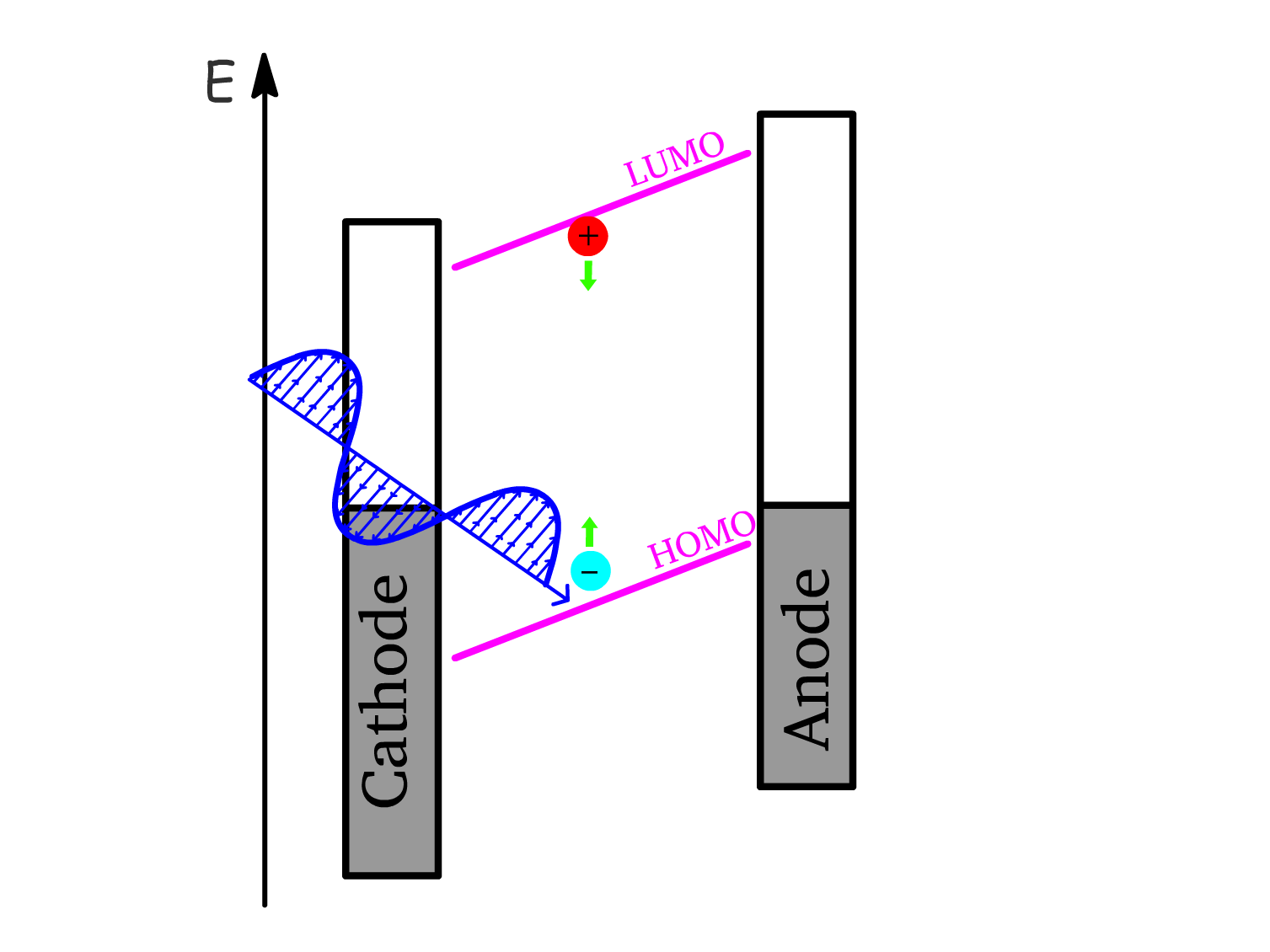
- Photon absorption within the semiconductor excites electrons from the HOMO to LUMO to create an exciton
2. Exciton Dissociation:

- The excitons are separated into free electron and hole polarons.
- This is usually achieved at the donor-acceptor interface of the semiconductor
3. Charge Transport:
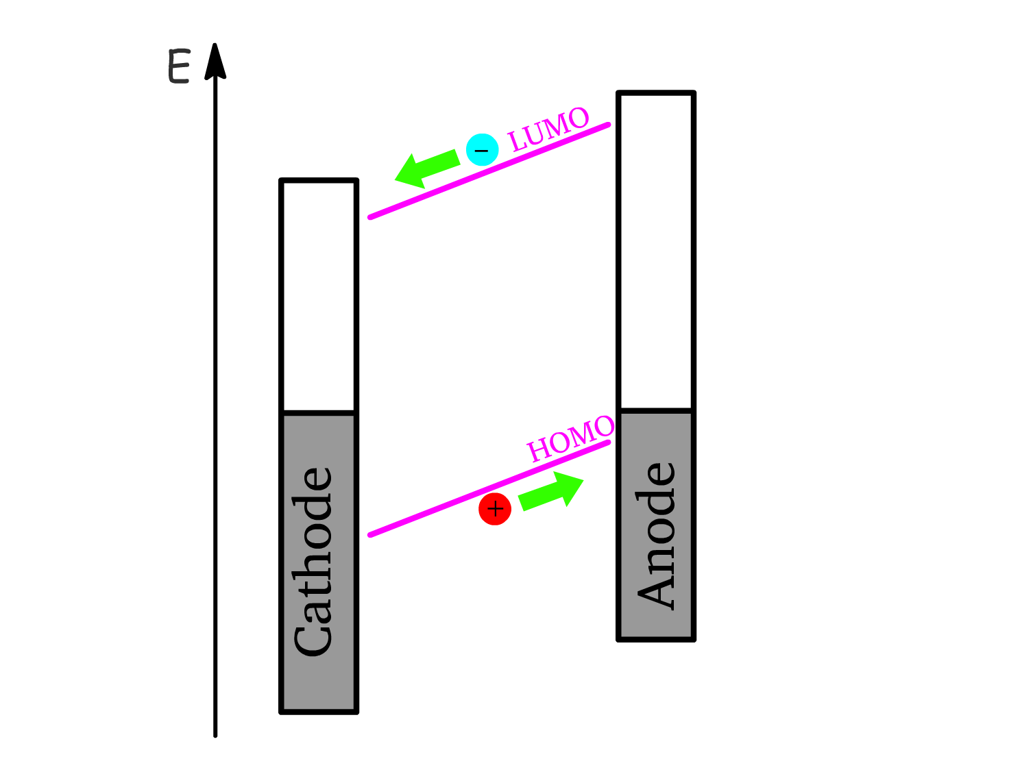
- The free electrons and holes are then transported through the semiconductor toward their respective electrodes.
- Electrons move toward the cathode, and holes move toward the anode, driven by the potential difference between electrodes.
4. Charge Collection:
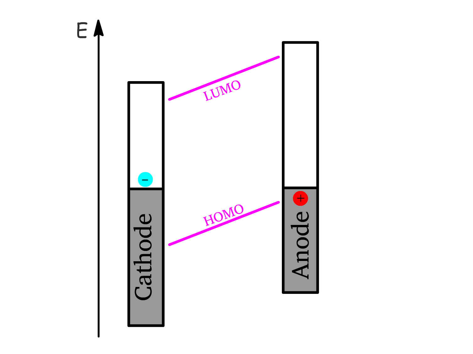
- Electrons are collected at the cathode and holes are collected at the anode.
- The flow of electrons and holes to their respective electrodes generates an electric current, which can be harnessed as electrical power.
Two Extreme Cases: Short-Circuit and Open-Circuit
A solar cell functions as a power source in a simple electric circuit, similar to how a battery operates.
- When the solar cell is illuminated, it produces voltage and current that can power devices with a load resistance ()
Extreme Case 1: Short Circuit ()
The electrodes of the solar cell are held at the same potential, meaning the terminals are connected directly to each other, and the resistance () is zero. In this scenario:
- Maximum current flows through the circuit.
- The electric field across the electrodes reaches its maximum value:
The relationship between short-circuit current density () and light intensity in a solar cell is given by
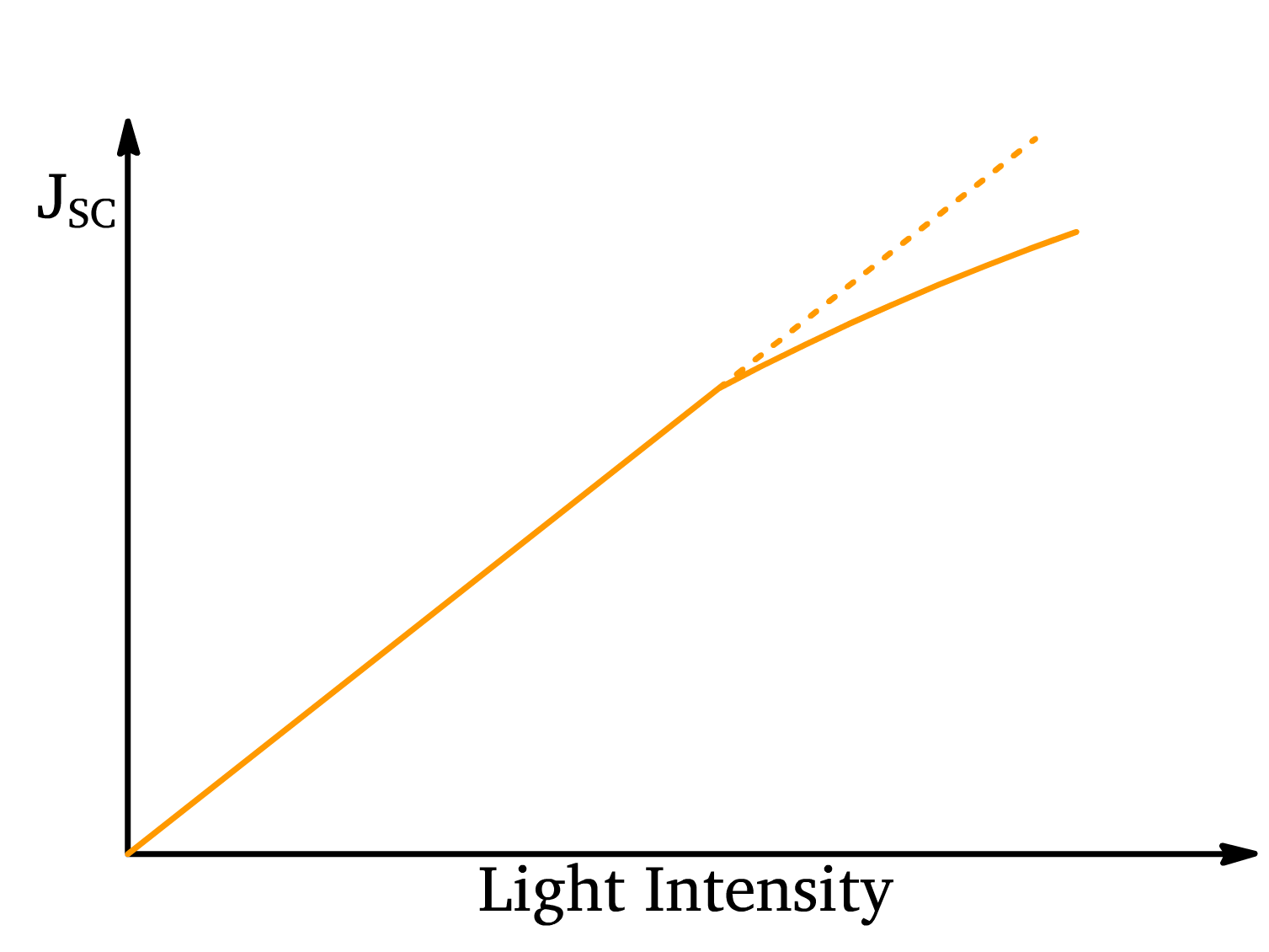
- Initially, as light intensity increases, the short-circuit current density increases linearly. This is because the number of absorbed photons (and therefore the number of excitons generated) is directly proportional to the intensity of the incident light. As more photons are absorbed, more excitons are created, leading to a corresponding increase in current.
- As the light intensity continues to rise, deviation from linearity occurs. This deviation is due to exciton-exciton interactions. At high intensities, there are so many excitons generated that they start to interact with one another. These exciton-exciton interactions can lead to recombination before the excitons can dissociate into free charges (electrons and holes). This results in a saturation effect in the short-circuit current, where the increase in current becomes sub-linear compared to the light intensity.
- Therefore, there’s a limit to how much current can be generated by increasing light intensity, and will start to plateau as these excitonic losses become more significant.
Extreme Case 2: Open Circuit ()
The electrodes are isolated (disconnected), meaning no current flows through the external circuit. In this scenario:
- The photocurrent is 0.
- The maximum voltage () develops across the device.
As the light intensity increases, the photovoltage initially increases linearly but eventually saturates as it approaches the
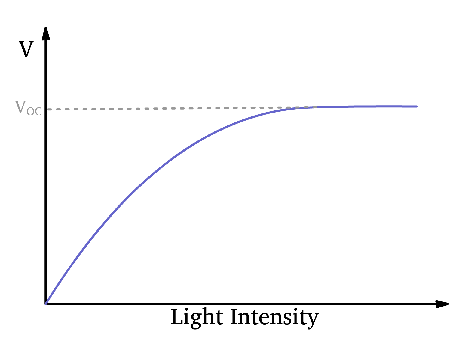
- At low to moderate light intensities, photons create excitons, and the electric field caused by the workfunction difference between the cathode and anode separates the charges, leading to a linearly increasing photovoltage as light intensity rises.
- As more charges accumulate at the electrodes, the semiconductor’s energy levels become less slanted, weakening the electric field and reducing the efficiency of charge separation.
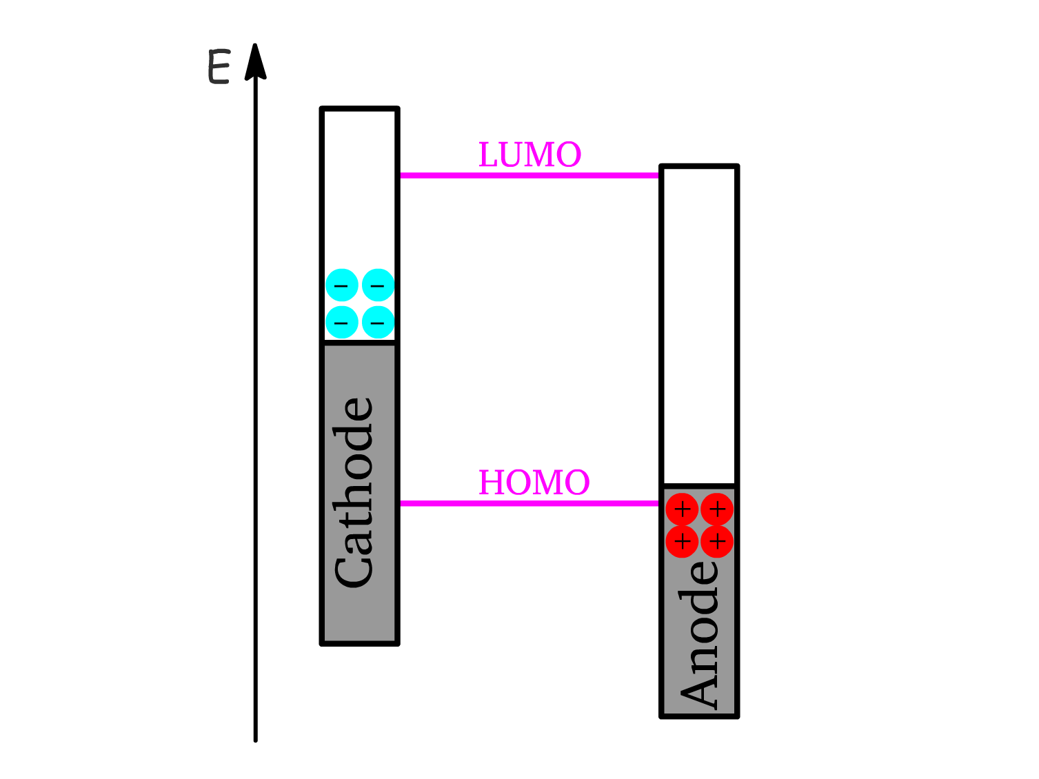
- At high light intensities, charge accumulation flattens the energy bands, reaching the flat band condition where charge separation is no longer favorable, causing the photovoltage to saturate at the maximum value determined by the workfunction difference ().
Intermediate Case
When a solar cell is used to power a device with intermediate load resistance (), the behavior of the photovoltage and photocurrent lies between the extreme cases of open-circuit (maximum voltage, no current) and short-circuit (maximum current, no voltage).
Photovoltage:
- The working photovoltage is less than the open-circuit voltage ().
- This occurs because the electrodes are connected to the external circuit, allowing charges to flow from one electrode to the other, which reduces the photovoltage from its maximum value at open-circuit conditions.
- The flow of charges between the electrodes diminishes the potential difference, hence reducing the working voltage.
Photocurrent:
- The working photocurrent is less than the short-circuit current.
- Unlike in the short-circuit condition, the electrodes are not held at the same potential. Therefore, a potential difference develops between the electrodes, which in turn reduces the electric field inside the solar cell.
- The weakened electric field reduces the efficiency of charge separation, resulting in a lower photocurrent compared to the short-circuit case.
Power Output:
- For an intermediate load resistance , the solar cell generates a working voltage () and delivers a working current () such that:
- The power output of the solar cell is given by:
- This power output is always less than the product of the short-circuit current and the open-circuit voltage:
J-V curve
The current-voltage (J-V) curve describes the behavior of a semiconductor device under varying voltage conditions. It represents different operating modes for devices like OLEDs and photovoltaic cells.
OLED (Semiconductor in the Dark)
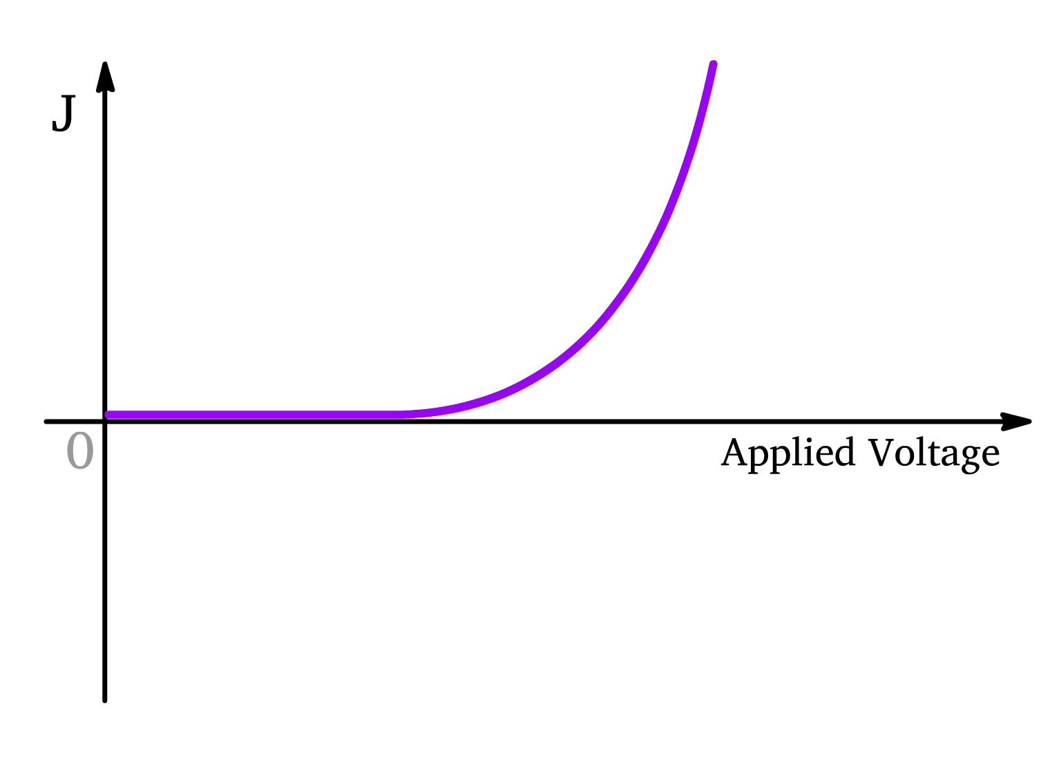
- At first, without sufficient applied voltage to generate a strong forward bias, there is no current flow since the energy band of the semiconductor is tilting towards the cathode
- As voltage surpasses the threshold of the flat-band condition, the energy levels of the semiconductor starts slanting such that it is tilted towards the anode. The polarons can now move across the junction, and current starts to flow.
- The current has a positive sign which means that the current (which is the flow of positive charge, by convention) towards the cathode and the electron moves toward the anode
Solar Cells (Semiconductor under Illumination)
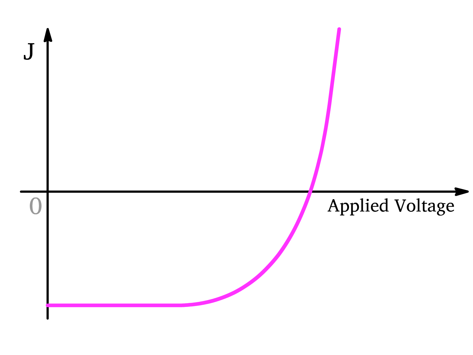
- When the applied voltage is 0, the device generates its maximum current (). The negative current indicates that the photocurrent flows from the anode to the cathode and the electrons flow from towards the cathode.
- As the applied voltage increases, the internal electric field is weakened, causing a decrease in current magnitude. This is because the external voltage counteracts the built-in electric field, slowing down carrier collection.
- When the voltage reaches the open-circuit voltage (), the internal electric field is neutralized, and the current becomes zero.
- As the applied voltage continues to increase beyond , the device begins to behave like an OLED. The external voltage drives carriers across the junction, causing current to flow in the opposite direction, and the device emits light rather than generating electricity.
Balance between the Opposing Process
As mentioned before, a good OLED can be repurposed to be a good solar cell. This means that when a solar cell is operating, both process are occuring
- To obtain the net current under light illumination, we have to account for both process
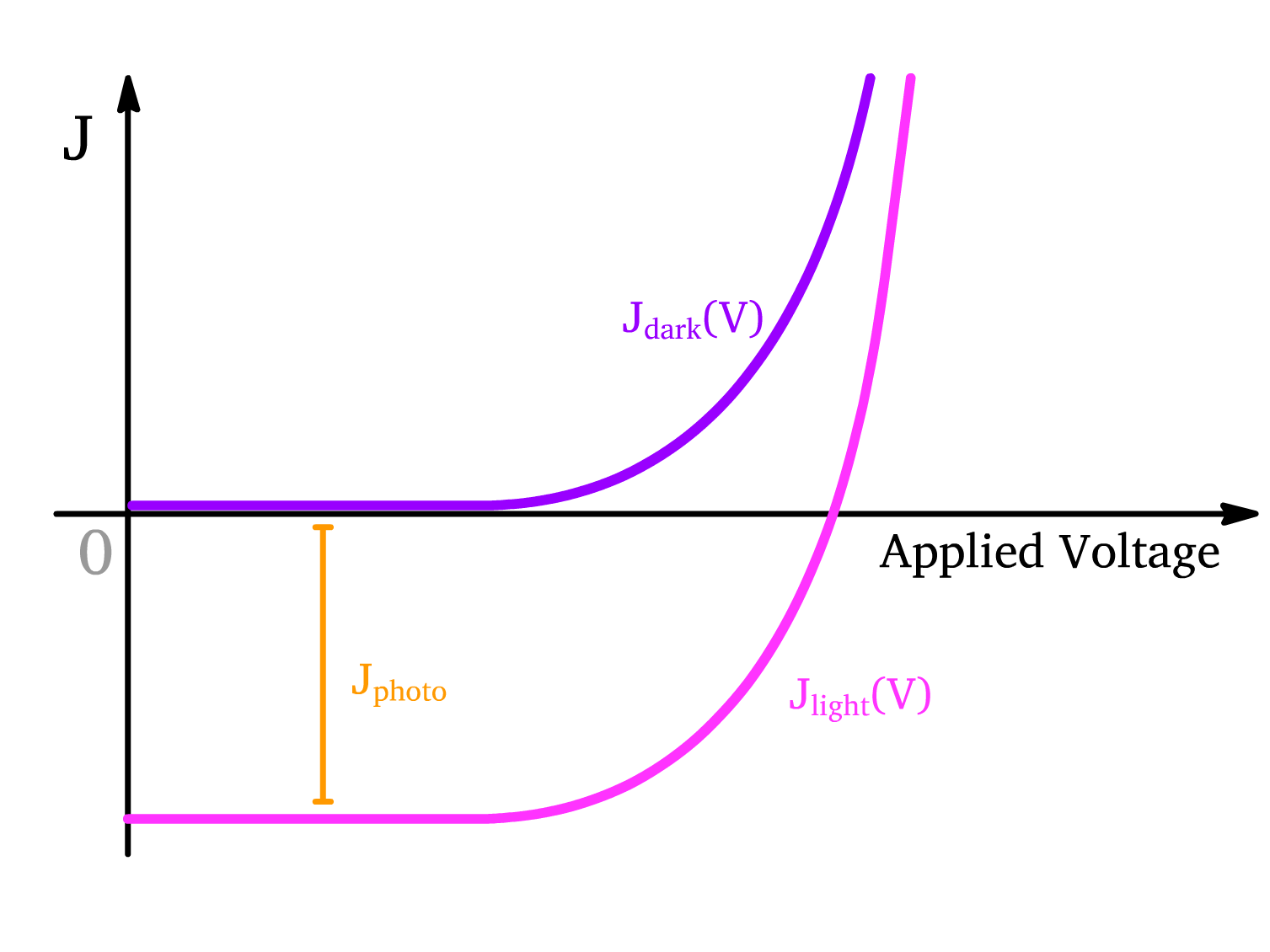
- The vertical distance () between the two curves shows how much current the solar cell generates due to light at any given voltage. The larger the vertical gap, the more efficient the device is at generating current from light.
Note that in inorganic solar cell, can be
understood by consideration of p-n junction
- But this expression DOES NOT WORK with perovsikes or organic semiconductors because charge recombination (which is present in perovsikes and organic semiconductors) is not accounted for in this equation
Power
The power output of the solar cell can be found by multiplying the voltage and the current (), which will produce a power curve
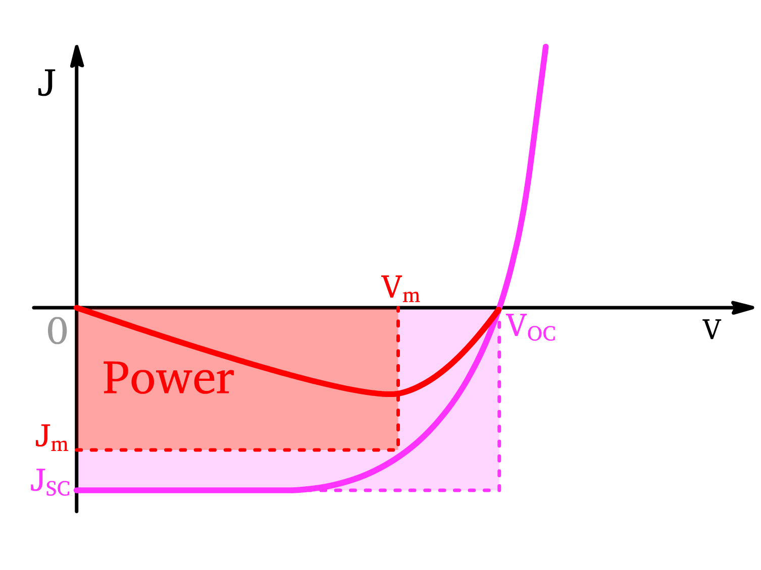
- We denote the current density and voltage corresponding to the maximum power as and respectively
The Fill Factor (FF) is a measure of how "square" the J-V curve is, indicating the efficiency of the solar cell in converting light to electrical power. It is defined as:
- The closer the fill factor is to unity, the more efficient it is
Power conversion efficiency () measures how effectively the solar cell converts the incident sunlight into electrical energy.
- is the incident power from the light
- This efficiency can be determined under standard solar illumination or monochromatic light, depending on the test conditions.
Photocurrent
- : The incident photon flux, which refers to the number of photons in an energy range () per unit area per unit time.
- represents the probability of converting a photon to an electron when the photon is in an energy range (). It is desirable to have a high QE at wavelengths where the solar flux density is high
We can express as
- is the probability that a photon will be absorbed, which depends on the thickness and absorption properties of the material. We can enhance it with thick material and use materials with high (extinction coefficient)
- is the probability of dissociation of excitons into free charge carriers.
- is the probability of the polarons reaching the device contacts without recombining
The exciton dissociation probability is usually quite low in organic layers
- Most excitons in organic layers are Frenkel excitons, with the polarons tightly bound together, making exciton dissociation challenging.
- The fraction of excitons with energy higher than the binding energy can be estimated using Boltzmann statistics, expressed as:
Where ( N_o ) is the number of excitons, and ( E_B = 0.4 \text{eV} ).
Donor-Acceptor Interface and Bilayer Solar Cells
One way to improve the probability of exciton dissociation is by using two different semiconductors.
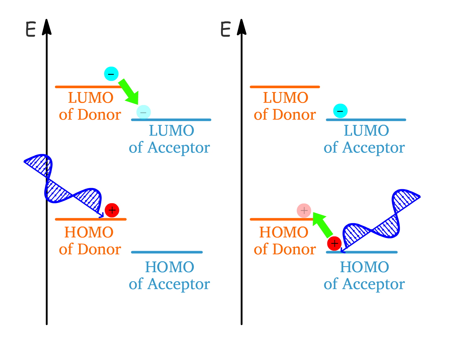
The semiconductor with LUMO and HOMO of higher energies is the Donor and the other is the acceptor
- When an exciton is formed on the donor, the electron polaron can jump down to the LUMO of the acceptor, thus splitting the exciton
- When an exciton is formed on the acceptor, the hole polaron can jump up to the HOMO of the donor, thus splitting the exciton
The exciton diffuses toward the interface, where charge separation occurs due to differences in the LUMO and HOMO energy levels between the two semiconductors.
- The separated charges are transported toward their respective electrodes (electrons to the cathode and holes to the anode) due to the electric field generated by the electrodes.
- The maximum cell voltage is determined by the energy gap between the lowest LUMO and the highest HOMO.
Limitations
The exciton generation follows an intensity profile given by:
- Light is absorbed as it travels into the material. The deeper the light goes, the less intensity remains to generate excitons.
- Most of the light is absorbed near the surface, and this absorption decreases exponentially with depth.
The ratio of excitons dissociating to total excitons generated is given by
- The probability of exciton dissociation decreases exponentially as the distance from the interface increases.
Hence, the key limitation is related to exciton diffusion length.
- In a bilayer device, excitons need to reach the donor-acceptor interface to separate into free charges. The problem is that excitons formed too far from the interface may recombine before they can reach it.
- Excitons have a limited lifetime and can only diffuse about 10 nm before they recombine, limiting the thickness of the active layer. Hence, only excitons generated close to the interface contribute to the photocurrent, and this spatial limitation impacts the overall efficiency of the bilayer device.
- To absorb sufficient light, the device needs to be thick, but excitons generated far from the donor-acceptor interface may not reach it before recombining.
The Bulk Heterojunction Concept
One way to overcome to aforementioned dilemma is through the bulk heterojunction concept
- It is an interpenetrating networks of donor and acceptor materials, creating a distributed (D/A) interface throughout the device.
- All excitons are generated close to the D/A interface, typically within
While the increased surface area promotes charge separation, it also raises the risk of interfacial recombination, where electron-hole pairs recombine before contributing to current.
Material Consideration
Polymer Donor
Polymer Band Gap and Efficiency: The band gap of a polymer, which depends on its HOMO level, plays a critical role in determining light absorption and efficiency. Efficient polymers generally have:
- Narrow Band Gaps: These polymers absorb a broader range of light, including infrared, converting more photons into excitons and, subsequently, electrical current.
- Push-Pull Hybridization: Combining electron-rich (donor) and electron-deficient (acceptor) units within polymers allows for tuning the band gap, enhancing light absorption and shifting absorption toward longer wavelengths (infrared).
We can thus use these properties in balancing and
- Reducing the Donor Band Gap
- Improves by enhancing light absorption and converting more light to current.
- However, this comes at the expense of , which is linked to the difference between the LUMO of the acceptor and the HOMO of the donor:
- Increasing the LUMO Energy of the Acceptor:
- This strategy raises but must be controlled carefully to maintain a ~0.3 eV offset between the LUMO levels of the donor and acceptor, ensuring efficient exciton splitting and charge separation.
- A similar balance applies to HOMO levels, requiring careful tuning to avoid reducing
Acceptor Material Considerations
For around 25-30 years, PCBM was the dominant acceptor in organic photovoltaics.
- Structure: Fullerene cage functionalized with ester groups for solubility.
- Key Properties: High mobility and a LUMO level of ~4.0–4.2 eV, making it compatible with polymer donors that have higher LUMO values.
Limitations of PCBM
- Poor light absorption, with a peak at ~400 nm.
- Low LUMO energy.
- Photoinstability under light exposure (Under nitrogen conditions, PCBM transforms into a dimer within ~40 hours of light exposure.)
- Limited capacity for structural modification and tunability.
New generation of acceptor: A-D-A (Acceptor-Donor-Acceptor) Non-Fullerene Acceptors
- Synthetic Flexibility: The ability to tune the HOMO, LUMO, and bandgap by substituting different units offers a high degree of customization for optimizing electronic and optical properties.
- High-Lying LUMO Levels: This leads to a higher open-circuit voltage (Voc) in devices, enhancing their overall efficiency.
- Strong Optical Absorption: Due to the pronounced push-pull electronic structure, these NFAs exhibit strong light absorption, making them effective at harvesting light energy.
- Cost-Effective Synthesis: The synthesis processes for NFAs can be relatively inexpensive compared to some traditional materials.
- Excellent Morphological Stability: This ensures better stability and performance over time, reducing degradation and maintaining efficiency.
Optimizing Fill Factor
There are three main things that affect fill factor:
- Charge carrier mobility (how quick the charges are extracted)
- Charge recombination processes( How slow they recombine)
- Active layer morphology (how well the donor acceptor material mixed together in the blend)
Active layer morphology
The morphology of the active layer in organic photovoltaic (OPV) devices is critical for achieving high efficiency. It must strike a balance between effective photon-to-current conversion and the ability to extract generated charges efficiently.
- A well-mixed donor-acceptor promotes efficient exciton dissociation since excitons typically have short lifetimes and diffusion lengths
- For efficient charge extraction, continuous pathways (percolation channels) must be present for electrons and holes to travel to their respective electrodes. In a morphology that is too well-mixed, these percolation pathways can be disrupted or too disordered, causing charges to become trapped or recombine before reaching the electrodes
Charge carrier mobility
Organic semiconductors inherently possess a lower charge carrier mobility compared to inorganic materials.
- This is primarily due to their disordered molecular structure, unlike the more organized lattice structures found in inorganic crystals like silicon.
- Organic materials typically form through Van der Waals interactions, resulting in amorphous or semi-crystalline structures, which hinder efficient charge transport.
Mobility is defined as the ratio of the average velocity of charge carriers to the applied electric field (), expressed as:
- Charge carriers in disordered organic materials are often strongly localized to a single molecule.
- Charge transport occurs primarily through a hopping process from one localized state to another.
The Poole-Frenkel equation describes how mobility changes with electric field:
- Here, is the zero-field mobility and is a constant characterizing the material's response to an electric field.
Magnitude of mobility is affected by:
- Polaron binding energy (energy needed to move a charged particle).
- The average distance between sites (affecting how easily charges hop between locations).
- Mobility in these materials is thermally activated, meaning it can change with temperature.
The experimental measurement of mobility employs the Time-of-Flight (ToF) method. In this technique, a light pulse (laser) generates charge carriers on one side of the organic film. These charges then drift across the film towards the opposite electrode under the influence of an applied electric field. The movement of the charges is tracked by measuring the photocurrent as a function of time.
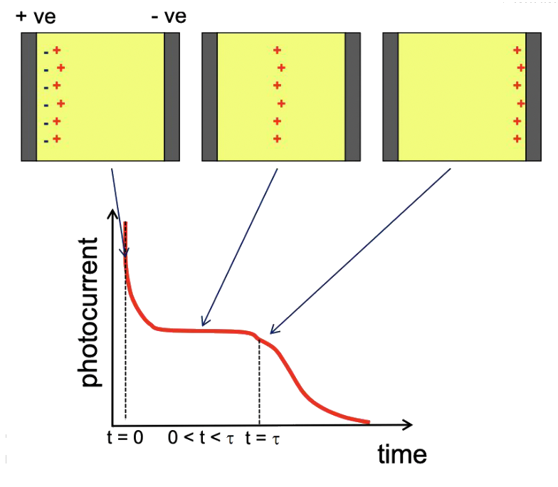
- Initially, there is a sharp increase in photocurrent as the charges are created, followed by a plateau representing a steady state as the charges travel through the film. The photocurrent eventually drops once the majority of the charges reach the opposite electrode.
- The mobility is calculated using the equation , where is the thickness of the organic film, is the transient time taken by the charges to travel through the film
Charge recombination processes
In bulk heterojunction (BHJ) solar cells, two key recombination processes influence the efficiency of charge separation and transport
- Geminate recombination occurs when an electron-hole pair, generated at the donor-acceptor interface, recombines without separating into free charges.
- This process is typically limited to the proximity where the pair was created.
- Non-geminate or bimolecular recombination happens when free electrons and holes, which have already separated, encounter each other within the bulk of the material and recombine.
- The recombination constant (indicates frequency of charge recombination) is determined by the slowest moving carriers
- The recombination process is typically limited by the carrier with the lower mobility, as it slows down the overall transport and extraction of charges. Therefore, reflects the slower carrier, which essentially controls how quickly charge recombination occurs in the system.
The presence and effect of space-charge formation is caused by unbalanced mobilities of electrons and holes.
- If one charge carrier moves significantly faster than the other (unbalanced mobility), it can lead to an accumulation of one type of charge, creating a space-charge region.
- This effect enhances recombination rates and reduces the fill factor.
- On the other hand, achieving balanced mobilities between electrons and holes ensures more efficient charge extraction, leading to reduced recombination and higher fill factors, thereby enhancing the device's efficiency.
Perovskite Solar Cells
Perovskites adopt an structure
- represents an organic or inorganic cation
- represents a metal cation
- represents a halide ion
Perovskite advantages over organic semiconductors
- Thick, printable devices: Perovskite solar cells can accommodate thick active layers (above 100 nm), making them suitable for printable technologies, whereas organics typically require thinner layers.
- Low binding energy: Perovskites generate free charges at room temperature due to their low exciton binding energy, eliminating the need to dissociate excitons, unlike organic materials that typically produce bound excitons.
- Longer diffusion length: Perovskites offer significantly larger diffusion lengths compared to organic semiconductors, enhancing charge transport efficiency and reducing recombination losses.
- Crystalline morphology: Perovskite materials are crystalline, enabling ordered charge transport and high carrier mobility, which contrasts with organic semiconductors that often possess amorphous or semi-crystalline structures, leading to disordered transport, low mobility, and lower photovoltaic performance.
Perovskite structures need specific ionic radii, described by the Goldschmidt tolerance factor :
- Ideal cubic lattice: Achieved when , ensuring optimal contact between B-site cations and X-site anions.
- Stability is maintained when ; values outside this range may lead to unstable perovskite structures.
Perovskite materials, being a hybrid structure of organic and inorganic components, exhibit four key interactions that influence their band gap and charge transport properties:
- Electrostatic interactions
- Dipole–Dipole interactions: These take place between the organic cations
- Charge–Dipole interactions: This interaction is present between the PbX cage and the organic cation
- Induced dipole interactions: These occur within the PbX lattice
Tuning X composition (, , )
Valence band is determined by the overlap of the 6s-orbital of and np-orbital of , so adjusting the halogen primarily affects the valence band.
- Larger anions result in, larger dipole interactions, reduced thermal stability, smaller lattice constants and narrower bandgap
- Excessive incorporation of results in -value dropping below 0.9.
Tuning B composition (, , )
-site elements influence conduction band energy.
- Increasing the size of B widens the band gap.
:
- Stability issues in the presence of oxygen due to oxidation from to .
- Known to introduce p-type self-doping, leading to high monomolecular electron-hole recombination and poor solar cell performance.
\text{Ge}^
- Instability caused by structural distortion.
- Assumed iodide spheres in Ge-based perovskites collide, destabilizing the symmetric structure.
- Poor t-value stability.
Here are the notes based on the provided slides regarding perovskite strategies and cation influence:
Influence of Organic Cation ()
Limitations:
- Hygroscopic and volatile; causes degradation and phase transition under ambient conditions (moisture, oxygen, heat, light).
- Results in limited long-term stability.
Strategies for Improving Stability:
- Cation Replacement ( and )
- Benefits: Improved thermal stability
- Drawbacks: Phase instability ; Polymorphs in both FAPbI₃ and CsPbI₃ (cubic, tetragonal, orthorhombic) leads to low photovoltaic performance.
- Double Cation Strategy ( and ). Pure FAPbI₃ phase is difficult to obtain.
- Mixed FA + MA perovskites yield better efficiency compared to pure FA or MA.
- Adding MA stabilizes the perovskite phase via I-H bonds due to a 10x larger dipole in MA compared to FA.
- Advantages: (MA)ₓ(FA)₁₋ₓPbI₃ insertion into the lattice stabilizes the α-phase ; Narrower bandgap ; Improved crystallinity enhances stability.
Issues: MA⁺ remains hygroscopic and volatile, making α-phase stabilization temporary ;
- Triple Cation Strategy (Cs⁺ Addition)
- (Cs)ₓ(MA)ₓ(FA)₁₋ₓPbI₃ structure eliminates photo-inactive hexagonal δ-phase, reducing effective cation radius for stable cubic α-phase.
- Results in higher thermal stability.
¶ Designing Organic Semiconductors
Semiconductors used in electronic devices are typically fabricated as thin films to ensure efficient charge transport and integration into compact systems.
Additionally, many applications require multilayer structures, where different semiconductors are layered to achieve specific electronic properties or device functionalities.
Based on fabrication methods, organic semiconductors can be categorized into two broad classes:
- Vacuum-Processable Semiconductors
- Solution-Processed Semiconductors
¶ Transistors
A transistor is a device that controls current output using a voltage input. It provides a current proportional to the applied voltage, allowing precise regulation of electrical signals.
¶ Metal-Oxide-Semiconductor Field-effect Transistor
The MOS structure is a typical multi-layered design fundamental to modern electronics.
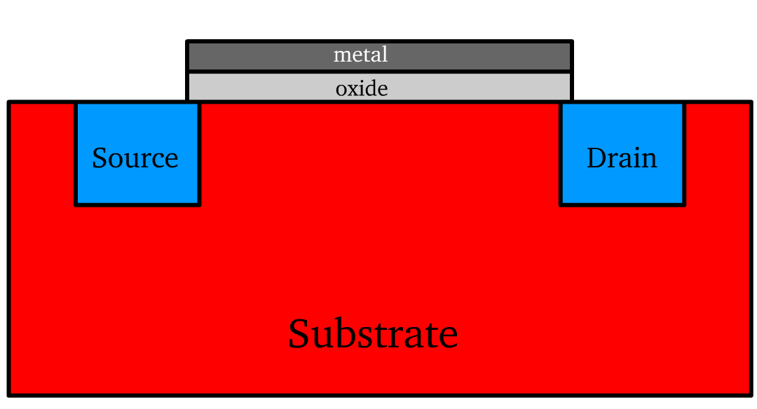
The substrate serves as the foundational semiconductor layer in the transistor. It is doped to create either a p-type or n-type material.
- Source and Drain Terminals: These are semiconductor regions doped opposite to the substrate, enabling charge injection and collection.
- The nature of the device (n-channel or p-channel) is the same as the doping of the terminals
The gate terminal is an electrode that modulates the channel that governs current flow. It is a conducting material positioned atop a thin layer of oxide, forming the core of the metal-oxide-semiconductor (MOS) structure.
- It is essentially a parallel plate capacitor, where the metal acts and silicon substrate act as plates and the oxide serves as the insulating medium.
- By applying voltage to the gate, the doping and type of charges (electrons or holes) in the channel region can be controlled, turning the transistor on or off.
The device is inherently symmetrical, meaning the roles of the source and drain terminals can interchange depending on the applied voltages.
- In the case of n-channel devices, the drain is defined as the terminal with the highest voltage relative to the source. Similarly, for p-channel devices, the polarity is reversed, and the source has the higher voltage relative to the drain.
- When there is zero gate bias (no voltage applied to the gate), the region under the gate does not form a conductive channel. Instead, this region behaves as two back-to-back diodes, with the source and drain terminals forming p-n junctions with the substrate. These junctions block current flow between the source and drain, ensuring no conduction in the absence of a gate-induced channel.
The MOS capacitor
The three components of the MOS capacitor are each defined by their energy levels
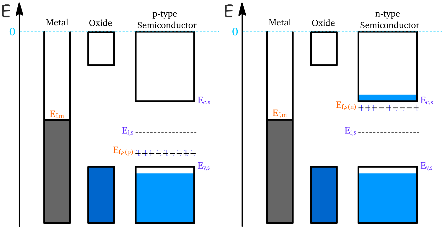
- When the components are not touching, their Fermi energy level need not be aligned and are defined by the product of charge times their work function ()
Upon contact between the metal and the semiconductor, the Fermi levels of the two materials must align to achieve thermal equilibrium. This alignment is accomplished by adjusting the Fermi level of the semiconductor or through charge redistribution.
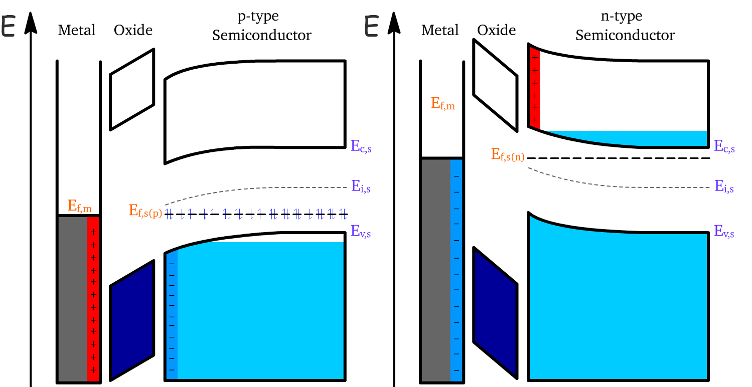
- This process results in a bending of the energy bands. However, since no chemical changes occur, the bandgap of the semiconductor remains constant
- This band bending modifies the doping behavior near the oxide interface. Specifically, the intrinsic energy level approaches the Fermi level ( ), effectively causing the material near the oxide to behave like an intrinsic semiconductor.
The change in doping near the surface occurs due to the redistribution of charge carriers:
- For p-types, electrons from the metal migrate toward the semiconductor surface and recombine with the holes in the valence band, forming a layer of negative charge
- For n-type semiconductors, electrons from the conduction band are lost to the metal, forming a layer of positive charge
Since holes and electrons recombine near the surface, the majority carriers essentially deplete from the interface
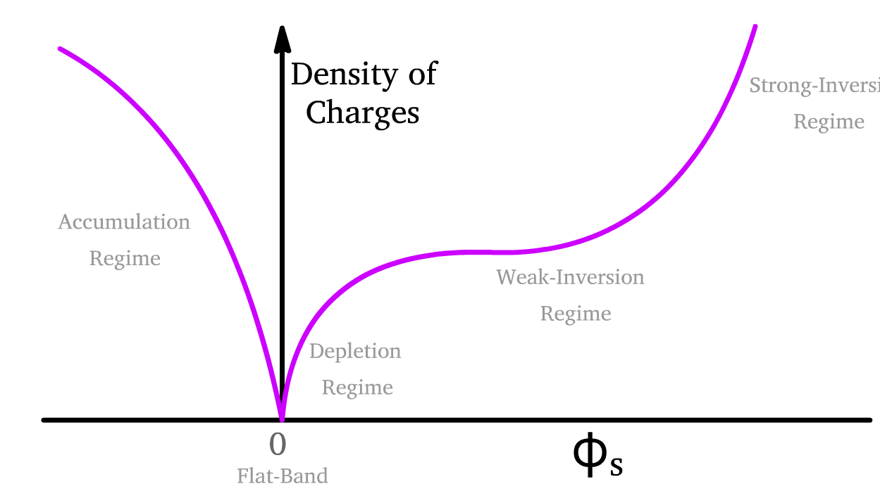
- We therefore call this operating region the depletion regime
There are two important potentials
- The flat band potential ( ) is the voltage needed to resist the built-in electric field generated to align the energy bands back to the original configuration and is defined by the difference in work functions
- The semiconductor surface potential is the difference between the intrinsic energy level of the semiconductor in the bulk and the surface
The device transitions into the accumulation regime when we go past even the flat-band condition and really resist nature
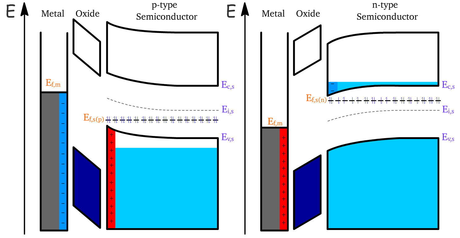
In the accumulation regime, a significant layer of majority carriers (holes for p-type semiconductors, electrons for n-type semiconductors) is drawn to the surface of the semiconductor near the oxide interface.
- This accumulation results in a reversal of the charge layer
The bending of the energy bands also reverses, leading to a flip in the sign of the surface potential (\phi_s).
- For p-type semiconductors: When a sufficiently negative gate voltage is applied, becomes negative, as holes accumulate near the surface.
- For n-type semiconductors: When a sufficiently positive gate voltage is applied, becomes positive, as electrons accumulate near the surface.
The magnitude of increases with the applied gate voltage, causing a stronger accumulation of majority carriers and deepening the accumulation region. This results in steeper energy band bending and enhances the charge density at the interface, further modulating the semiconductor's surface properties.
If we double down on the depletion regime, we will actually transition into the inversion regime
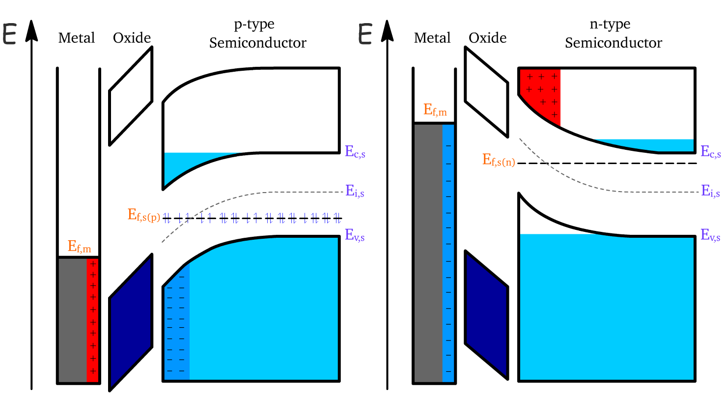
At this regime, the bending is so extreme that the intrinsic Fermi energy level of the semiconductor passes the actual Fermi level
- This means that near the oxide interface, the doping of the semiconductor essentially reverses. And since the two terminals are also oppositely doped, it essentially opened up a channel to connect the two
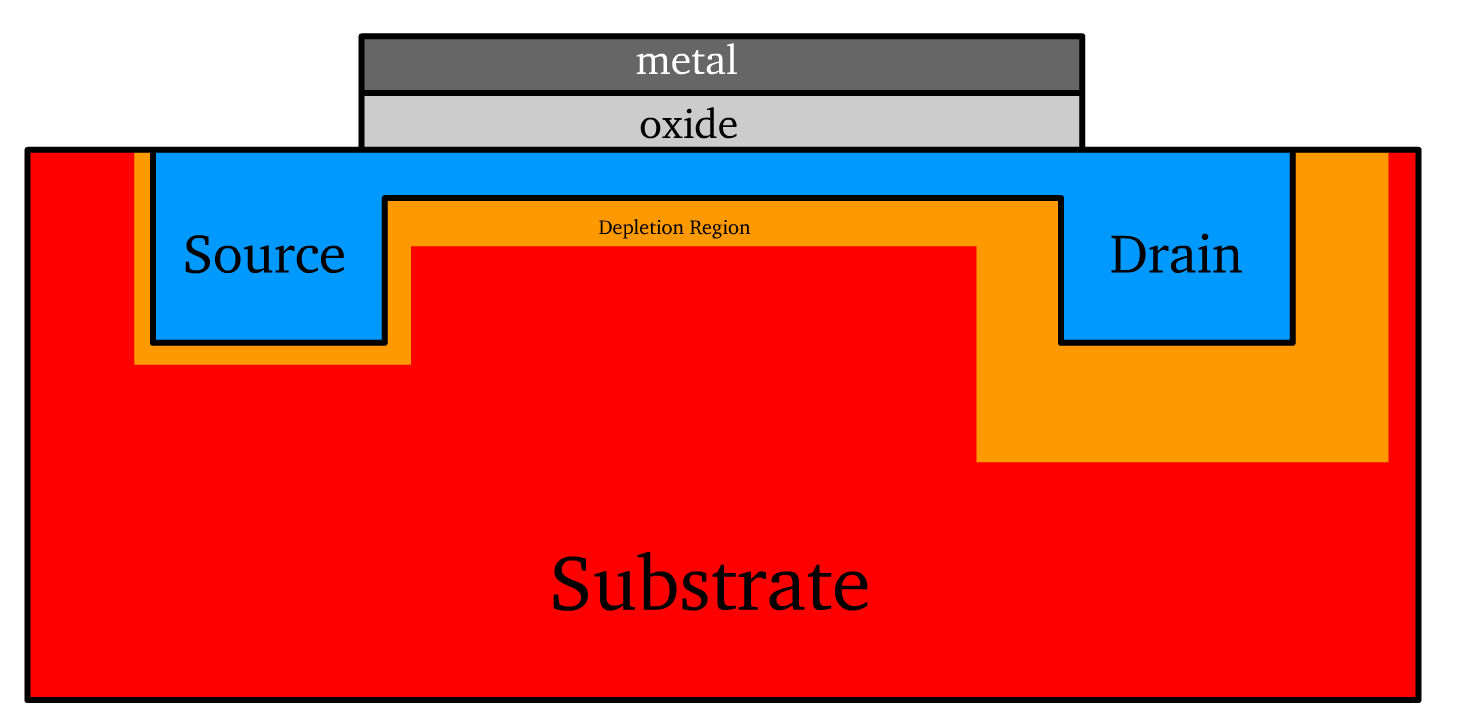
- The critical voltage required to form a conductive channel and enable current flow between source and drain is called the threshold voltage V_\text
There are two types of inversion regimes
Summary of the Four Regimes of MOSFET Operation:
Gate Voltage vs Terminal Voltage
The gate voltage plays a critical role in determining the "width" of the channel formed between the source and drain terminals in a MOSFET.
- A higher gate voltage attracts more charge carriers to the surface of the semiconductor near the oxide interface, effectively widening the channel.
- The width of this channel directly impacts the current flowing between the source and drain, with a wider channel allowing for a higher current.
Simultaneously, the voltage applied between the terminals also influences the current.
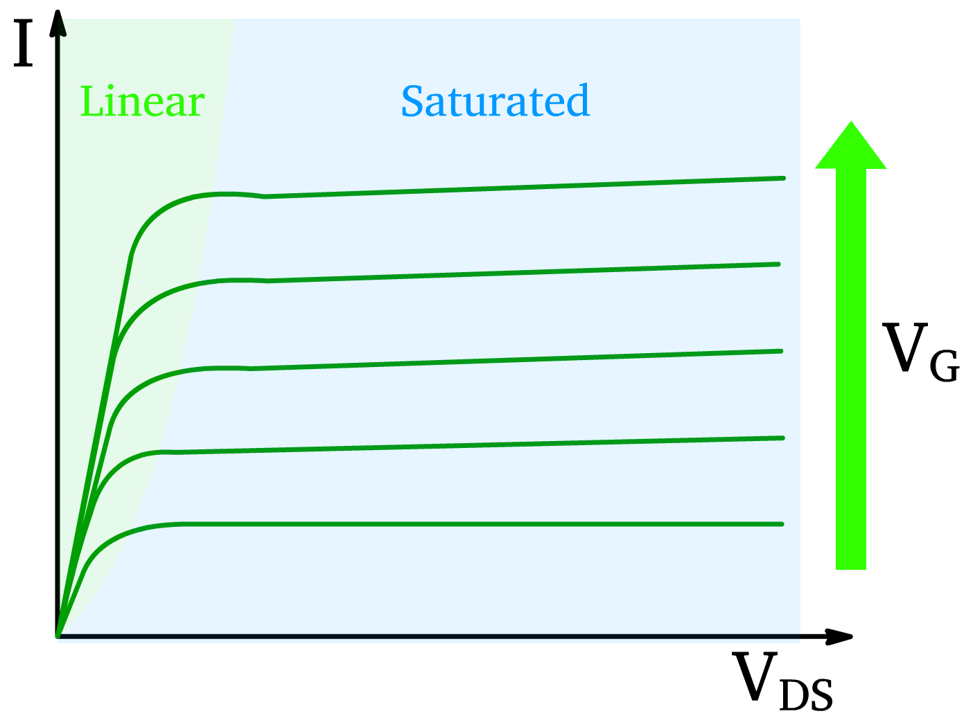
- Initially, increasing results in a higher drain current, as it drives the carriers from the source to the drain through the channel.
- However, as increases, it also expands the depletion region near the drain terminal, effectively "pinching" the channel and narrowing its width.
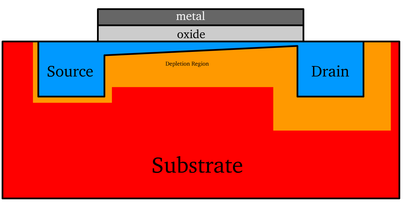
- However, the channel can never be narrowed to the point of completely closing because the gate voltage continues to attract charge carriers to the channel, maintaining a minimum conductive path. This phenomenon defines the saturation current, where the current is now limited by the rate at which carriers are injected into the channel from the source.
¶ Thin Flexible Transistor
Thin Film Transistors (TFTs) are a distinct class of transistors that differ significantly from traditional inorganic MOSFETs.
- TFTs function primarily in the accumulation region. This is because organic TFTs often exhibit limited mobility for both electrons and holes, making charge carrier inversion uncommon
- Furthermore, while the substrate in MOSFETs is an active component of the device, in TFTs, the substrate is electrically inert and serves solely as a mechanical support
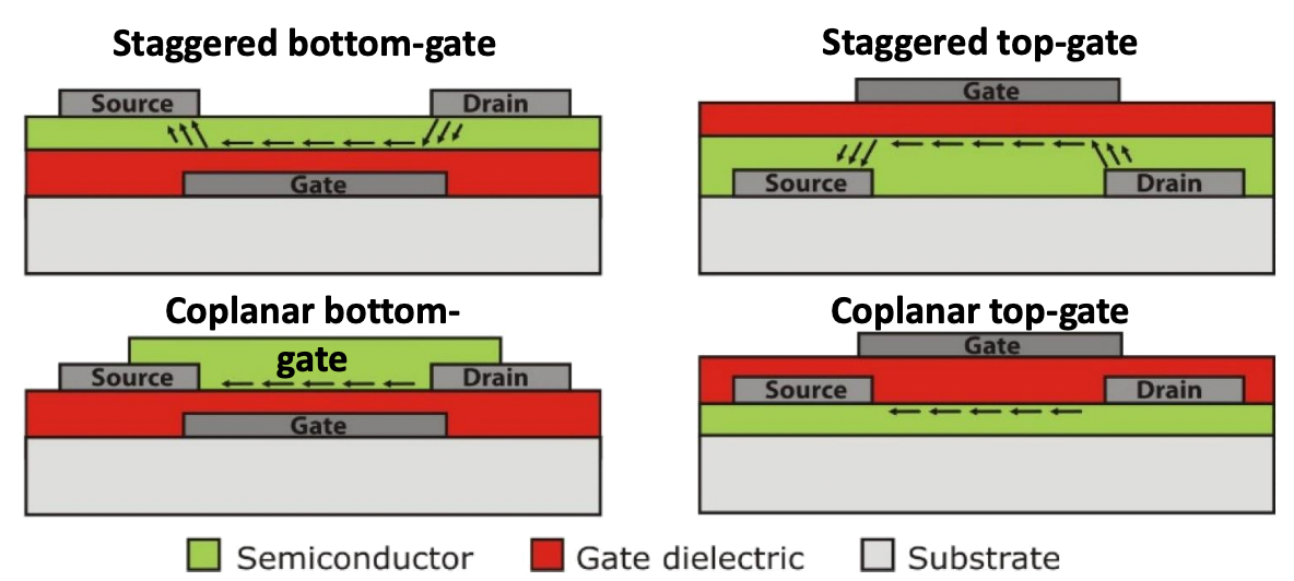
TFT layouts can be categorized along two axes of properties: structural configuration (coplanar vs. staggered) and gate orientation (top-gate vs. bottom-gate)
Structural Configuration
- Coplanar Structures
- Electrode and Dielectric Positioning: The source/drain electrodes and the dielectric are located on the same side of the channel.
- Applications: Typically used in high-temperature semiconductors, as the uniform structure supports better heat tolerance during fabrication.
- Staggered Structures
- Electrode and Dielectric Positioning: The source/drain electrodes and the dielectric are located on opposite sides of the channel.
- Applications: Commonly implemented in bottom-gate layouts when high-temperature dielectric layers are necessary for device functionality.
Gate Orientation
- Top-Gate Configuration
- The gate electrode is positioned above the channel.
- Often paired with coplanar layouts in devices requiring high-temperature semiconductors for enhanced compatibility.
- Bottom-Gate Configuration
- The gate electrode is positioned below the channel.
- Frequently paired with staggered layouts in applications where high-temperature dielectric processing is critical.
Schottky Barrier
A Schottky barrier arises at the metal-semiconductor interface due to the difference in work function between the metal and the semiconductor.
- Unlike pn-junctions found in MOSFETs, the Schottky barrier lacks a depletion region and thus offers inferior blocking properties especially when it is thin
The terminal voltage primarily regulates the flow of charge carriers between the source and the drain, creating a potential difference across the semiconductor channel
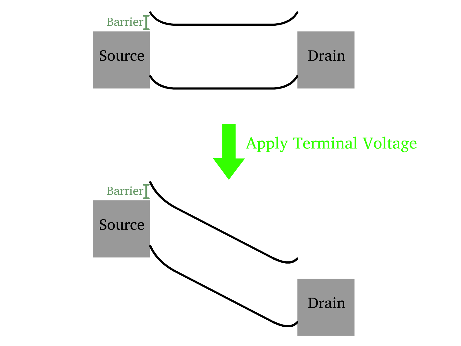
- In the transistor’s off-state, the Schottky barrier is responsible for minimizing leakage currents by preventing charge carriers from easily traversing the barrier.
The gate voltage is responsible for inducing and controlling the accumulation of majority carriers at the semiconductor/oxide interface, as TFTs primarily operate in the accumulation regime.
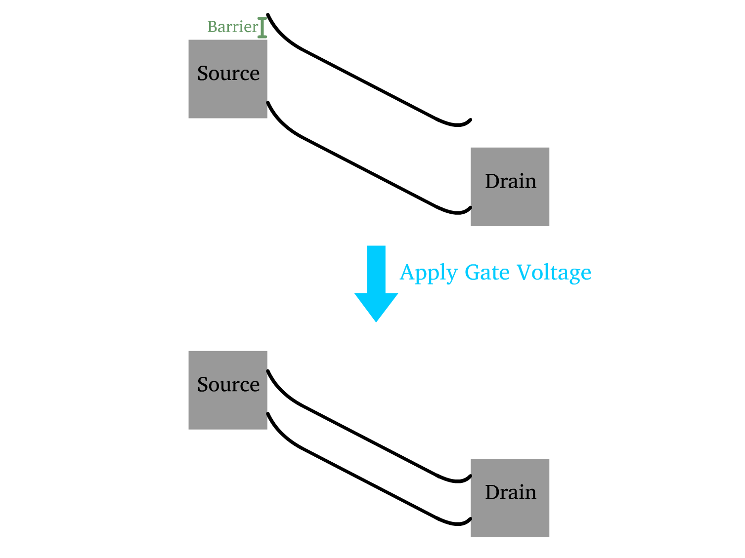
- When a voltage is applied to the gate electrode, it reduces the width of the Schottky barrier at the source and drain terminals.
- This barrier narrowing facilitates the flow of charge carriers, thereby increasing the drain current.
- As the barrier width decreases further, the device transitions to the on-state, where majority carrier transport dominates.
Charge Transport and Current in Transistors
The Drude model provides a foundational understanding of charge transport in transistors. It assumes free electrons behave like a classical gas, colliding with stationary ions rather than with one another. The key relationships are:
- Drift Velocity () due to an electric field ()
- Conductivity
- Electron Mobility
- Current Density
Current in the linear region \bm
In the linear region, when the gate voltage exceeds the threshold voltage , a conductive channel forms between the source and drain. Here:
- The drain voltage controls the current and defines the electric field across the channel .
- The current increases linearly with as long as .
The drain current in the linear region is:
Current in the saturation region \bm
When approaches , the channel near the drain narrows due to an increasing depletion region.
- The channel pinches off, and current saturates.
- In this saturation region, the current becomes independent of (V_d).
The drain current in the saturation region is given by:
Due to the high density of majority carriers accumulated by the TFT operating in accumulation mode, the linear-saturation transition is smoother than in MOSFET.
The key difference between inorganic and organic transistors lies in the unique behavior of organic semiconductors, where the conjugated polymers are stacked layer by layer.
- In these materials, the voltage experienced by each layer is not uniform, as each layer absorbs a portion of the applied voltage.
- This contrasts with inorganic transistors, where the voltage distribution across the material is more uniform.
To account for this voltage distribution in organic semiconductors, the total surface charge density is expressed as a sum over all layers:
- : Surface charge density of the (i^{th}) layer.
- : Capacitance of the insulator
- : Gate voltage applied.
¶ Vacuum-Processable Semiconductors
These semiconductors are typically insoluble in most solvents, so the only way to create thin films is through sublimation in a high-vacuum environment.
Advantages:
- High Purity: Ionic contaminants can be readily removed during the sublimation process.
- Precise Thickness Control: Sublimation allows for meticulous control over the thickness of the film
- Multilayer Feasibility: The sublimation technique makes it easy to deposit multiple semiconductor layers without concern for interlayer mixing
Disadvantages:
- High Cost: Equipments and maintaining high-vacuum environment are expensive
- Low Throughput: The process is inherently slow, making it challenging to scale up for large-area
Molecular Design
The reliance on sublimation entails that the material needs to overcome intermolecular forces during the heating process. This imposes specific molecular design requirements:
- Low Molecular Mass: Molecules must typically have a molecular mass ≤ 1000 g/mol to sublimate efficiently.
- No Entanglement: Polymers are not suitable for vacuum processing as their long chains entangle, preventing sublimation.
- Stable Bonding: Fragile bonds (e.g., solubilizing groups) must be avoided. Molecules are usually entirely sp²-hybridized, providing rigidity and thermal stability.
- Poor Solid-State Stacking: Poor molecular packing in the solid state can lower intermolecular forces, facilitating sublimation.
¶ Solution-Processed Semiconductors
These semiconductors can be dissolved in solvents, enabling thin films to be created through techniques like spin-coating, inkjet printing, or roll-to-roll processing.
Advantages:
- Printable and Scalable: Compatible with scalable manufacturing techniques, making them suitable for large-area applications
- Cost-Effective: Relatively inexpensive equipment and have lower operational costs
Disadvantages:
- Purity Concerns: Achieving high purity is challenging, especially for polymers, as ionic impurities from synthesis are difficult to remove.
- Multilayer Challenges: When creating multilayers, the solvent used for the top layer can disrupt or mix with the underlying layers. Additionally, achieving uniform surface wetting without interlayer contamination requires careful control of material properties and processing conditions.
Further Classification
Solution-processed semiconductors fall into two main categories:
1. Small Molecules
- Easy Purification and Characterization: The uniformity of small molecules allows for easier purification and characterization, critical for maintaining consistency in device performance.
- No Entanglement: Small molecules' lack of entanglement contributes to high solubility and low viscosity, enabling easy solution preparation. However, this high solubility creates challenges in multilayer processing, as solvents can dissolve or disrupt the underlying layers.
- Brittle Nature: Small molecules are generally brittle, limiting their mechanical durability in flexible devices.
2. Polymers
- Limited Solubility: Polymers tend to have lower solubility compared to small molecules
- Excellent Rheology: Polymers exhibit good flow properties, making them ideal for printing and coating processes.
- Toughness and Flexibility: Polymers are mechanically robust and flexible, making them suitable for flexible and wearable electronics.
- Challenges with Purity: Polymers are polydisperse, meaning their molecular weights vary, which complicates purification and characterization.
Making Soluble Semiconductors
Creating soluble semiconductors involves modifying the materials to enable solution processing while maintaining their electronic properties. Two primary routes are used, each with its advantages and challenges.
Route 1: Chemical Reactions on a Soluble Precursor
Process:
- Begin with an organic semiconductor that is insoluble and non-printable.
- Modify it into a soluble precursor, usually by disrupting its conjugation.
- Deposit and print the precursor layer.
- Perform a reaction (e.g., thermal or chemical treatment) on the printed layer to restore its conjugated structure and semiconductor properties.
Advantages: Enables multilayer processing by ensuring the precursor is compatible with underlying layers.
Challenges:
- Requires high temperatures, which may damage the material or substrate.
- Achieving film perfection after post-processing can be difficult.
- Solution rheology (flow behavior) may complicate printing, as the precursor's properties may not be optimized for consistent deposition.
Route 2: Adding Sidechains to Increase Solubility
Process:
- Introduce sidechains to the conjugated core of the organic semiconductor.
- The sidechains disrupt van der Waals interactions, enhancing solubility by increasing entropy in solution or melt states.
Sidechains Also Influence Solid-State Packing
- Charge mobility: Poor packing can hinder charge transport.
- Bandgap width: Packing changes may alter electronic properties.
- Phase segregation: Interactions between sidechains can lead to structural separation within the material.
Molecular Design
The performance and properties of organic semiconductors are influenced by multiple factors that affect their band gap, charge mobility, and other electronic characteristics. Below are six main factors:
Factor 1: Effect of Conjugation Length
Bandgap Reduction with Longer Conjugation:
- As conjugation length increases, the bandgap decreases.
- However, structural distortions (Peierls distortion) occur, pairing and localizing single electrons, causing the bandgap saturates at effective conjugation length (~n=35).
Controlling Conjugation:
- Introducing non-conjugated linkers or cross-conjugated linkers can limit conjugation to tune electronic properties.
Chain Length and Mobility:
- At low molecular weights, polymers may form crystalline structures with poor inter-crystallite packing, resulting in low mobility.
- At high molecular weights, amorphous structures with tighter packing facilitate charge hopping and improve mobility.
- Aim for high molecular weight and low dispersity to ensure reproducibility and optimal performance.
Factor 2: Backbone Planarity
Backbone Twisting:
Sidechain insertion affects planarity:
- Head-to-head insertion creates more non-planar backbones.
- Tail-to-tail insertion results in planar backbones.
Controlling Torsion:
- Ring fusion: Adding a bridging unit restricts rotation, reducing energetic disorder, increasing rigidity, and improving emission properties.
- Non-covalent interactions: Planarizing forces, such as H-bonding, can stabilize backbone geometry and improve orbital overlap.
Factor 3: Backbone Chemistry
Electron-Withdrawing or Donating Groups:
- Adding EWG or EDG modifies both the HOMO and LUMO levels without significantly affecting the bandgap width.
- However, deeper HOMO levels increase , enhancing device efficiency.
Factor 4: Co-Polymerisation
Donor-Acceptor (D-A) Hybridization:
- Co-polymerizing electron-rich monomers (D) with electron-poor monomers (A) results in molecular hybridization.
- Since the energy difference between D and A is large, the orbital mixing is weak, so the resultant HOMO and LUMO levels remain close to those of the original (Homo of D ; LUMO of A)
- This enables independent tuning of HOMO and LUMO levels to achieve desired bandgap widths.
- Outcome: Reduced bandgap, enhanced optical absorption, and better charge transport.
Factor 5: Heteroatom Effects (S vs Se)
Heteroatoms Influence LUMO:
- Heteroatoms like sulfur (S) or selenium (Se) contribute to LUMO energy levels.
- The larger size of Se facilitates charge hopping, improving mobility.
- Inductive effects from heteroatoms also impact the HOMO level, affecting charge transport and stability.
Factor 6: Excited State Stabilization
Stabilizing the LUMO
- Stabilizing the Excited State lowers the LUMO energy and narrows the band gap
- One example is the quinoidal resonance, where aromaticity is formed from the pro-aromatic ground state
¶ Transport in Conducting Polymers
Conductivity and Mobility in Polarons
In certain materials with specific doping levels, the Fermi level resides within the conduction and valence bands.
- The motion of polarons is therefore linked to the response of phonons (crystal lattice vibrations) to the electric field.
- This coupling leads to scattering events with phonons, making the transport process fundamentally different from the free electron motion observed in inorganic crystals.
The conductivity of polarons can still be described using Drude's theory:
The mobility of charge carriers in an ideal crystal is governed by its dependence on temperature and is expressed as:
- This highlights the inverse proportionality between mobility and temperature
- The exponent depends on the nature of scattering mechanisms in the material.
Mobility can also be expressed using the diffusion coefficient as follows:
- The diffusion coefficient is further defined as:
As temperature increases:
- Phonon activation: More phonon modes are activated, causing stronger polaron-phonon interactions.
- Mean free path reduction: Increased phonon scattering reduces the mean free path , as charge carriers interact more frequently with lattice vibrations.
- Shorter scattering time: The time between successive scattering events decreases due to intensified thermal vibrations.
This directly impacts the diffusion coefficient and, consequently, mobility. The result is a unique property observed in organic polymers:
- This temperature-dependent behavior reflects the distinct transport mechanisms in organic systems, where lattice vibrations play a significant role in limiting carrier mobility.
Child's Law: Current Density in Conjugated Polymers
Child's law provides a framework for understanding how internal charge dynamics affect current flow in materials like conjugated polymers.
- While Ohm's law ( ) assumes the ideal case that across the material is uniform and unaffected by the material's internal charge distribution, the situation changes when internal charges within the material become significant.
- This is particularly important in organic semiconductors, where charge mobility and screening effects strongly influence device performance.
As the total charge in the material becomes comparable to the electrode charge, the internal charges begin to screen the applied field.
- now follows Child's law, which accounts for how the material's charges modulate the electric field
Traps in Organic Semiconductor
Traps play a crucial role in limiting the mobility and current density of charge carriers in organic semiconductors.
- These are localized states, often associated with impurities or structural defects, that act as energy wells where charges can get trapped
- Traps contribute to the screening of the electric field, further reducing the current density
Traps are regions in the material where charges are stored temporarily.
- These traps are thermally activated, meaning that charges can escape if sufficient thermal energy is provided.
The mobility of charge carriers is strongly affected by the energy depth of the traps ():
Charges are fixed and do not contribute to the net current flux.
- However they affect the surroundings by contributing to the space charge.
- The in the Child’s law can be replaced by an effective mobility ( ) given by
¶ Graphene
Band Structure of Graphene
The unique properties of graphene stem from its distinct band structure, which is neither metallic nor semiconducting.
In the plot, the valence and conduction bands of graphene overlaps at discrete points called Dirac points.
- At these points, the energy of the valence band and conduction band is equal, creating a gapless band structure.
The Fermi level of graphene resides in the middle between the conduction and valence bands, called the charge neutrality point.
- At theese points, there are no free electrons in the conduction band or holes in the valence band.
Close to the Dirac points, the relationship between energy and is linear instead of the typical parabolic relationship seen in semiconductors.
- This leads to quasiparticles that mimic massless Dirac fermions instead of electrons with an effective mass.
Electrostatic Doping of Graphene
One of the most effective ways to explore and manipulate the electrical properties of graphene is through a thin-film transistor configuration.
- Unlike traditional semiconductors, graphene exhibits a highly tunable resistivity due to its unique low charge density and linear band structure.
When a gate voltage is applied to a graphene sheet in a thin-film transistor, the resistivity of graphene exhibits a sharp, non-linear change.
- It increases dramatically from near-zero to a high value and then drops back to near-zero.
- This behavior corresponds to a conducting-to-quasi-insulating transition, which occurs as the Fermi level crosses the charge neutrality point.
Graphene's unique low charge density places the Fermi level very close to the CNP, where the density of states is minimal. Hence, applying a gate voltage can move the Fermi level:
- Above the CNP: Graphene becomes n-doped (electron-dominated)
- Below the CNP: Graphene becomes p-doped (hole-dominated).
Graphene's low intrinsic charge density is the key to its tunability
- In the ideal case, the intrinsic charge density at the CNP is zero.
- The Fermi level sits at the intersection of the valence and conduction bands, enabling rapid modulation with minimal voltage.
- This contrasts sharply with semiconductors, where changing doping levels involves altering the material's chemical composition.
The relationship between gate voltage and charge carrier density in graphene can be described using the capacitance formula:
- Unlike traditional materials, the charge carrier density in graphene is directly proportional to the applied gate voltage.
- This enables precise tuning of graphene's electrical properties
Optical Properties of Graphene
Graphene is remarkably transparent, the transmittance and absorbance of a single graphene layer is given by:
- is the fine structure constant, this means that its transmittance and absorbance is constant and independent of scattering effects
Liquid Phase Exfoliation of Graphene
Liquid-phase exfoliation is a scalable and low-temperature technique to disperse layered materials like graphene into solvents, producing printable inks suitable for processable electronics.
- Unlike methods like mechanical cleavage, this technique prioritizes processability over exceptional quality, making it highly relevant in applications requiring large-scale production.
How Liquid Phase Exfoliation Works
- Initial Material:
- Start with layered materials such as natural graphite
- Disperse the material into a solvent
- Energy Input:
- Apply mechanical forces such as:
- Rotor-stator mixing: A common industrial technique involving high-speed rotational shear.
- Ultrasonic exfoliation: Utilizing high-frequency sound waves to break apart layers.
- Resulting Dispersion:
- The layered material laminates into thin graphene sheets, forming a dispersion that can be processed into printable inks if the rheology is optimized.
The stability of graphene dispersion in solvents is determined by minimizing the Gibbs free energy of mixing ( ). For a spontaneous and stable dispersion, must be negative:
- Entropy Contribution: is generally small and often negligible for graphene dispersions.
- Enthalpy of Mixing: dominates and is proportional to the surface energy difference between the solvent ( ) and graphene ( ):
Key Condition for Stability: A close match between the surface energies of the solvent ( ) and graphene ( ) minimizes , ensuring a stable dispersion. This condition is expressed as:
In the process of liquid-phase exfoliation, the maximum concentration of dispersed graphene () is influenced by the surface energy mismatch between the solvent and graphene.
When dispersing graphene in water or polar solvents (where the surface energy does not match graphene), surfactants or polymers are used to stabilize the dispersion:
- Surfactants:
Surfactants like sodium dodecyl sulfate (SDS) provide stabilization by forming a dual-phase structure:
- This prevents graphene reaggregation and ensures dispersion in aqueous solutions.
- Polymers:
Polymers like cellulose are sustainable alternatives to surfactants.
- The hydrophilic phase of the polymer interacts with the solvent, while the hydrophobic phase adheres to graphene, maintaining a stable dispersion.
Transport in Graphene Networks
Graphene networks are composed of randomly oriented graphene In graphene networks, charge transport occurs primarily via hopping mechanisms, where charge carriers move between adjacent graphene flakes. The effectiveness of this hopping depends on the connectivity of the flakes:
- Disconnected Network: Limited transport as isolated flakes inhibit charge flow.
- Connected Network: At sufficient flake concentration or thickness, a continuous pathway forms, enabling percolation of charges and higher conductivity.
The transition from sparse connectivity to a continuous network occurs at the percolation threshold:
- Below this threshold ((t_c) or (X_c)), the flakes are not sufficiently connected, leading to poor conductivity.
- At and above the threshold, the flakes form a continuous network, allowing efficient charge transport through hopping mechanisms.
In a percolation regime, conductivity is proportional to the excess concentration of flakes above a critical threshold:
Similarly, conductivity scales with the excess thickness of the graphene film:
Below the Percolation Threshold or :
- Flakes are sparsely connected.
- Hopping pathways are limited or nonexistent, resulting in poor conductivity.
- Conductivity depends linearly on thickness or concentration but remains low.
Above the Percolation Threshold or :
- A continuous network forms, allowing efficient charge transport.
- Conductivity increases sharply and no longer depends significantly on thickness, transitioning to bulk conductivity.
Graphene Transistor (G-FET): Properties and Performance
Graphene’s unique electronic properties allow it to transition between p-type and n-type conduction:
This transition is governed by gate voltage, which tunes the Fermi level relative to the charge neutrality point.
At the charge neutrality point (also known as the Dirac point), the number of charge carriers approaches zero, resulting in minimal conductivity.
Moving the Fermi level below the neutrality point induces p-type behavior, while moving it above results in n-type behavior.
Graphene transistors exhibit unconventional characteristics when compared to traditional MOSFETs:
- Drain Current vs. Gate Voltage:
The relationship is non-linear due to graphene’s gapless band structure.
At the Dirac point:
- Conductivity reaches a minimum due to zero charge carrier density.
- Transition between electron (n-type) and hole (p-type) conduction occurs.
- Drain Current vs. Drain Voltage ((I_D = f(V_{DS}))):
The conventional linear and saturation regions seen in MOSFETs are not clearly defined in graphene.
Instead:
- A quasi-linear region appears at low drain voltages.
- Current plateaus but does not saturate due to graphene’s lack of a band gap.
- At higher voltages, a second linear region emerges, linked to graphene’s high mobility and unique conduction.
Graphene transistors exhibit a low ON/OFF ratio, making them unsuitable for switching applications.
- The absence of a band gap prevents clear transitions between fully conducting and fully insulating states, as seen in MOSFETs.
¶ Printed Electronics
Printed electronics involve the fabrication of electronic devices using wet deposition techniques.
- Functional materials are deposited in a layer-by-layer manner onto either flexible or rigid substrates, enabling the creation of lightweight, scalable, and cost-effective devices.
Printing electronic devices broadly consists of 5
primary phases:
- Device Conceptualisation
- Ink Formulation
- Substrate Preparation
- Deposition and Post-Deposition Treatment
- Characterisation
¶ Device Conceptualisation
This phase sets the foundation for developing printed electronic devices by defining the problem, conceptualizing solutions, and strategizing materials and components.
Problem Definition
- What? Define the problem or need the device addresses.
- Who? Identify target users and environments.
- How? Prioritize key features and constraints.
Concept Development
- Ideation: Develop design concepts (sketches, CAD, simulations).
- Feasibility: Evaluate practicality in terms of cost, materials, technology, regulations, and sustainability.
Material and Component Strategy
- Select materials aligned with performance needs (e.g., conductivity, flexibility).
- Ensure component compatibility for integration and scalability.
To streamline the design process and balance competing requirements, a structured framework is employed. Two main approaches include:
1. Design for Performance (DfP):
| Aspect | Design for Performance |
|---|---|
| Optimisation Scope | Maximising functional performance under specified conditions, often at the expense of complexity or cost. |
| Metrics | Meeting or exceeding performance metrics (speed, efficiency, reliability, durability). |
| Strength | Achieves Cutting Edge Performance. |
| Limitation | May not be feasible beyond proof of concept, or results in extensive cost premium. |
| Examples in Academia | Advanced material research, theoretical design optimisation. |
| Examples in Industry | Products demand peak performance (e.g., aeronautics, defence, space, certain healthcare applications). |
2. Design for Manufacturing (DfM):
| Aspect | Design for Manufacturing |
|---|---|
| Optimisation Scope | Minimise production costs and complexity while maintaining minimum performance metrics. |
| Metrics | Ensuring ease of manufacturing, assembly, and scalability. |
| Strength | Reduces costs, streamlines production, and shortens time-to-market. |
| Limitation | May limit product innovation and compromise optimal performance. |
| Examples in Academia | Proof-of-concepts, prototyping methods, manufacturing process studies, scalability assessments. |
| Examples in Industry | Mass-market products (e.g., consumer electronics, automotive assembly). |
¶ Ink Formulation
Ink formulation is a critical step in printed electronics, where functional materials are transformed into printable dispersions.
Ink Composition
Dispersion: A system consisting of two or more phases, where one phase is continuous, and at least one other is finely dispersed.
Ink: A processable material for printing that contains a functional material, fillers, binders, dispersants, and a dispersion medium or solvent.
Paste: A high-viscosity formulation used when thicker material deposition is needed.
Functional Materials
Functional materials in electronic inks serve as the primary active layer and are the core components that define the ink’s electronic properties.
- Conductive Inks: Facilitate the flow of electric current.
- Semiconductor Inks: Used in active electronic applications.
- Insulating Inks: Provide electrical insulation between conducting components.
Solvent
A good solvent possesses the following characteristics:
- Dissolves the functional material effectively.
- Does not degrade ink components or the substrate.
- Evaporates at a rate suitable for the printing process.
- Is compatible with the ink carrier system.
- Provides the desired viscosity and surface tension for deposition.
Co-solvents may be incorporated to fine-tune surface tension and drying rates.
Additives
Additives enhance the performance and stability of inks. Key types include:
- Filler: Improves physical, mechanical, or thermal properties.
- Binder: Adhesive components that ensure fillers and active materials adhere to the substrate post-deposition.
- Stabilisers: Prevent undesirable phenomena such as aggregation, sedimentation, and viscosity changes. They also preserve the ink's functional properties during storage and processing.
Rheology
Rheology is the study of the physical behavior of materials under stress, which is critical for understanding ink flow during deposition processes.
Viscosity ()
Viscosity is the resistance of a fluid to flow, and it is defined as
- Shear Stress ( ): Force applied per unit area, expressed as: \tau = \frac{F}
- Shear Rate ( ): Change in strain over time: , where , where is fluid displacement (mm), and is the gap between plates (mm).
Newtonian Fluids
Newtonian fluids have a linear relationship between shear stress ( ) and shear rate ( ), where viscosity ( ) remains constant regardless of shear rate.
Non-Newtonian Fluids
Non-Newtonian fluids exhibit a non-linear relationship between shear stress and shear rate, where viscosity changes with shear rate. These behaviors are categorized as follows:
- Shear Thinning (Pseudoplastic):
- Viscosity decreases as shear rate increases:
- Shear Thickening (Dilatant):
- Viscosity increases as shear rate increases:
- Bingham Plastic:
- Viscosity behaves like a solid until a certain yield stress ( ) is exceeded. Beyond this point, the fluid begins to flow, and the relationship between stress and flow becomes linear.
Surface Tension
Definition: Surface tension ( ) is the energy or work required to increase the surface area of a liquid due to intermolecular forces.
Behavior: It governs how liquids behave at interfaces, such as droplet formation and ink spreading on surfaces.
¶ Substrate Preparation
Substrate Identification
The substrate is the foundational layer upon which devices and components are built or fabricated. The substrate’s properties directly influence:
- Performance
- Longevity
- Usability of the final device.
Substrate properties also determine the deposition techniques used during fabrication (e.g. spin-coating or printing).
Surface Properties: Wettability
Wettability refers to the ability of a liquid to maintain contact with a solid surface, which results from intermolecular interactions between the liquid and substrate.
Measurement of Wettability:
- It is quantified using the contact angle ( ), which represents the angle a liquid forms with a substrate surface.
- A well-prepared substrate ensures uniform wettability, which is essential for consistent material deposition and device performance.
¶ Deposition Treatments
Pre-Deposition Techniques
Pre-deposition treatments are critical to preparing substrate surfaces for material deposition, ensuring cleanliness, improved adhesion, and optimized surface properties for device fabrication.
UV ozone treatment is a versatile pre-deposition process that serves two interconnected purposes: cleaning substrate surfaces and modifying surface energy.
Cleaning Substrate Surfaces:
- Ozone Generation:
- UV light at 185 breaks molecular oxygen () bonds, forming ozone ().
- Excitation of Organic Molecules:
- UV light at 254 excites organic contaminants, generating organic radicals.
- Reaction and Removal:
- Organic radicals react with ozone, producing volatile byproducts: , , that desorb, leaving a clean surface.
Substrates are then free of organic residues, enhancing their readiness for deposition.
Surface Energy Modification
- Contaminant Removal:
- Removes low-energy contaminants, exposing high-energy surfaces like metals and ceramics.
- Addition of Functional Groups:
- UV light breaks down into hydroxyl radicals that attach to the surface, increasing its energy.
Such modification can
- Improves material adhesion and wettability.
- Facilitates functionalization for advanced material deposition.
It should be noted that there is temporal limitation:
- Surface energy enhancements are temporary as organic recontamination can reduce the effect over time.
Wet Deposition Techniques
Production Line Considerations
The choice of production line directly impacts the efficiency, scalability, and precision of wet deposition techniques in electronic fabrication. There are three primary production approaches:
- Sheet-to-Sheet (S2S) Production:
- Process: Substrates are individually fed through the system for processing.
- Application: Ideal for rigid or semi-rigid substrates, commonly used in high-precision or small-volume production scenarios.
- Advantages: Offers greater control over the deposition process, resulting in higher precision.
- Reel-to-Reel (R2R) Production:
- Process: Continuous rolls of flexible substrates are processed through uninterrupted manufacturing steps.
- Application: Suitable for high-throughput production.
- Advantages: Highly efficient and well-suited for large-scale industrial applications.
- Batch Production:
- Process: Products are created in specific quantities within a defined time frame.
- Application: Often overlaps with S2S for small-scale production or R2R for defined production runs.
- Advantages: Practical for logistical or quality control reasons, enabling adjustments for smaller projects.
Printing vs. Coating in Wet Deposition
Printing and coating are two distinct methods for applying functional materials in wet deposition processes. Each has unique mechanisms and applications:
- Printing:
- Mechanism: Transfer of material via a patterning tool or stamp.
- Pattern Formation: Forms complex and detailed patterns on substrates.
- Techniques Examples: Inkjet, screen printing, gravure, and flexographic printing.
- Material Precision: Ensures high precision, making it suitable for detailed device designs.
- Applications: Used in functional device components requiring intricate patterns.
- Coating:
- Mechanism: Material deposition through spreading or smearing techniques.
- Pattern Formation: Typically results in uniform layers over large areas.
- Techniques Examples: Spin coating, Mayer rod coating, and spray coating.
- Material Precision: Provides consistent thickness and is ideal for large-scale coverage.
- Applications: Common for substrate preparation and bulk material deposition.
| Drop Casting | |
|---|---|
| Overview | Simple film-forming deposition technique requiring minimal equipment. |
| Process Steps | 1. Surface Preparation: Clean and prepare substrate. 2. Ink Deposition: Pipette ink onto substrate. 3. Evaporation: Allow volatile components to evaporate (ambient, vacuum, or heat). 4. Optional Repetition: Repeat process to build thickness. |
| Performance Parameters | Scale: Sheet-to-Sheet (S2S). Throughput: Lab-scale, highly variable. Resolution: Covers entire substrate; basic patterns achieved with tape/masks. Ink Viscosity: No strict restrictions. Wet Film Thickness: Typically in the micrometer (µm) range. |
| Strengths | - Minimal setup costs. - Quick and efficient. - Low material wastage. - Widely used in academia. - Accessible for small-scale experiments. |
| Limitations | - Poor film homogeneity. - Low resolution; limited pattern complexity. - Poor repeatability across depositions. - Requires planar substrates for optimal results. |
| Optimization Parameters | - Ink Properties: Tailor viscosity, surface tension, and boiling point. - Surface Properties: Adjust surface energy to improve wetting. - Process Conditions: Modify drying rates with heat or vacuum. |
| Applications | Used in academia and R&D for thin films of polymers or nanomaterials for electronics and optoelectronics. |
| Spin Coating | |
|---|---|
| Description | A technique used to produce uniform thin films by depositing a solution onto a rotating substrate. |
| Key Steps | 1. Substrate Loading: Substrate secured to the chuck (often using vacuum). 2. Deposition: Solution pipetted at substrate center. 3. Spin Up: Substrate rotates, expelling excess liquid. 4. Spin Off: Liquid thinning by centrifugal forces, with edge effects forming droplets. 5. Evaporation: Fluid outflow stops; film thickness determined by evaporation rates. 6. Spin Down: Substrate decelerated and removed. |
| Film Thickness Relationship | ( ; ) |
| Performance | Scale: S2S. Widely adopted in academia and industry. Throughput: Low, highly variable. Resolution: Coating entire surface; limited by edge effects. Ink Viscosity: Not limited. Wet Film Thickness: 10–100s nm. |
| Optimisation Parameters | Ink Properties: Viscosity, surface tension, boiling point. Spin Parameters: Speed, acceleration time, spin duration. Surface Properties: Cleanliness, adhesion. Deposition Variables: Droplet volume, static/dynamic deposition. Process Conditions: Drying rates, humidity, and airflow. |
| Strengths | - Low setup cost. - Quick (~30s for water, ethanol, IPA). - Produces very thin, uniform films. - Repeatable at high speeds (>1000 rpm). - Simple and widely used. |
| Limitations | - Low resolution (requires photolithography for fine patterns). - High material wastage (>90% spun off). - Slower turnaround time for prototyping compared to inkjet. - Restricted to planar surfaces. |
| Mayer Rod Coating | |
|---|---|
| Process | 1. Liquid Application: Liquid is dispensed in front of the Mayer rod as it is positioned on the substrate. 2. Film Formation: Liquid is spread across the surface through the coil gap, with grooves regulating thickness. 3. Levelling and Drying: Surface tension smooths out ridges, creating a uniform film. |
| Performance | Scale: Reel-to-Reel (R2R) Throughput: 10s–100s m/min Resolution: Entire surface coating, ~5–50 μm film thickness (down to 100s nm in academia) Ink Viscosity: 20–1000 mPa·s |
| Optimisation Parameters | Ink Properties: Viscosity, surface tension, boiling point Rod Specifications: Diameter, wire diameter, wire density Coating Properties: Rod movement speed, substrate feed rate Surface Properties and Process Conditions: Drying conditions |
| Strengths | - Straightforward setup - Good thickness control for thin films - Scalable |
| Limitations | - Contact-based technique - Slower turnaround for prototyping compared to inkjet - Restricted to planar surfaces - Low resolution (coating technique) - Streaking may occur |
| Screen Printing | |
|---|---|
| Process | Steps involved in Screen Printing: 1. Design your Screen: A screen or mesh is prepared with a stencil design. Non-printing areas are blocked using polymer masks or emulsion, leaving open mesh for ink passage. 2. Substrate Placement: Substrate is positioned below the screen with the aid of alignment markers. 3. Ink Loading: High-viscosity ink is placed at the top of the screen and spread using the squeegee. 4. Pattern Transfer: A scraper moves across the screen, causing the ink to pass through the open mesh, forming the desired pattern on the substrate. 5. Curing: Ink is dried or cured. |
| Components | Faceplate: Rigid frame supporting the mesh or screen. Screen (mesh): Woven fiber or metal mesh adhered to the frame, providing the stencil image for ink passage. Squeegee: Rubber blade spreading ink across the mesh. Scraper: Forces ink through the mesh while cleaning excess ink. Screen Masks: Polymer film sheets covering non-image areas for stencil creation. Printed Matter: Final product with ink deposited through the masked mesh. |
| Performance | Scale: Sheet-to-Sheet (S2S) and Reel-to-Reel (R2R). Throughput: Up to 160 m/min (highly variable). Resolution: >40 μm (usually 100s of μm). Ink Viscosity: 1000–10000 mPa·s. Wet Film Thickness: ~25 μm. |
| Optimisation Parameters | Ink Properties: Viscosity, surface tension, boiling point. Screen Design: Mesh count, mesh material, wire diameter, emulsion thickness. Surface Properties: Substrate type and treatment. Printing Properties: Squeegee hardness, speed, angle, and pressure applied. Process Conditions: Drying temperature, humidity, airflow. |
| Strengths | - Low setup costs. - Quick processing. - Widely adopted in academia and industry. - Low material wastage. - Adaptable for non-planar surfaces. |
| Limitations | - Prone to screen clogging and smearing. - Slower prototyping turnaround compared to inkjet. - Produces thick films. - Limited resolution. - Contact technique, requiring high-viscosity inks. |
| Rotary Screen Printing | A variation using cylindrical screens with perforations: 1. Perforated Cylinder: Utilized for ink transfer. 2. Ink Supply: Pump ensures continuous ink flow. 3. Ink Transfer: Cylinder rotation and squeegee force ink through perforations. 4. Multi-Screen Support: Supports complex designs. 5. High Throughput: Large-scale, consistent production in R2R format. |
| Equation | Thickness ( ) is determined by: Where: : Volume of ink per unit screen area (cm³/m²). : Pick-out ratio. : Solid concentration in ink (g/cm³). : Density of solid material in the film (g/cm³). |
| Direct Gravure Printing | |
|---|---|
| Process | 1. Substrate: Substrate passes between engraved printing cylinder and impression cylinder. 2. Ink Reserve: Engraved cylinder picks up ink from the reservoir. 3. Impression Cylinder: Transfers ink to substrate under applied pressure. 4. Doctor Blade: Removes excess ink, ensuring only the ink within wells remains. 5. Printing Plate: Engraved/etched directly on the cylinder, eliminating need for separate plates. |
| Forward vs Reverse Gravure | - Forward Gravure: Cylinder rotates in the same direction as substrate; directly transfers liquid. - Reverse Gravure: Cylinder rotates in opposite direction, increasing shear forces for improved quality. |
| Performance | - Scale: Industrial R2R with high throughput. - Throughput: 1000 m/min. - Resolution: >1 μm. - Ink Viscosity: 1–5000 mPa·s. - Wet Film Thickness: 1–25 μm. |
| Optimisation Parameters | - Ink Properties: Viscosity, surface tension, boiling point. - Engraving Parameters: Cell geometry, cell depth, lines per inch. - Surface Properties: Surface energy and roughness. - Printing Properties: Speed, applied pressure. - Process Conditions: Doctor blade angle, drying conditions, pressure. |
| Strengths | - Durable cylinders for low long-term costs. - Quick and widely adopted in industry. - Low material wastage. - Compatible with various substrates. |
| Limitations | - High initial setup cost. - Not ideal for prototyping; requires different plates for each design. - Requires technical expertise. - Contact technique; restricted to planar surfaces. |
| Flexographic Printing | |
|---|---|
| Description | A roll-to-roll (R2R) printing technique that uses flexible printing plates and cylindrical components to transfer ink onto a substrate. |
| Key Steps | 1. Ink Supply: Ink stored in a reservoir (tray). 2. Ink Pickup: Fountain cylinder rotates through the ink tray and transfers ink to the anilox cylinder. 3. Ink Regulation: Doctor blade scrapes excess ink from the anilox cylinder for uniformity. 4. Image Transfer: Flexible printing plate transfers ink to raised image areas. 5. Printing Action: Substrate passes between plate and impression cylinders, applying pressure for ink transfer. |
| Performance | - Scale: R2R - Throughput: Up to 300 m/min (highly variable). - Resolution: 50–100 µm. - Ink Viscosity: 100–50,000 mPa·s. - Wet Film Thickness: ~1–400 µm. |
| Optimisation Parameters | - Ink Properties: Viscosity, surface tension, boiling point. - Anilox Design: Cell volume, line count, cell shape, depth, material coating. - Surface Properties: Surface tension, cleanliness. - Printing Parameters: Speed, substrate tension, pressure applied. - Process Conditions: Drying rates, humidity. - Plate Specifications: Material type, plate thickness, relief depth. |
| Strengths | - Low setup cost compared to gravure printing. - Quick and efficient. - Widely adopted in academia and industry. - Low material wastage. - High-speed and high-volume production possible. |
| Limitations | - Not ideal for prototyping. - Contact-based technique. - Requires high-viscosity inks. - High initial setup cost for plates and cylinders. - Restricted to planar surfaces. |
| Inkjet Printing | |
|---|---|
| Overview | Inkjet printing is a non-contact technique that precisely propels ink droplets onto substrates to form patterns for applications like sensors. |
| Types of Inkjet Printing | Continuous Inkjet (CIJ): Continuous stream of ink droplets, charged, and directed. Drop-on-Demand (DoD): Droplets ejected as needed. |
| Key Components | Ink Reservoir: Stores ink. Nozzles: Eject droplets. Printhead: Deposits patterns on substrates. |
| Mechanisms in DoD | Thermal: Heats ink to form vapor bubbles. Piezoelectric: Uses electrical pulses to create pressure waves. EHD: High voltage generates fine droplets. |
| Strengths | High resolution, adaptable for thin films, minimal material wastage, and compatibility with complex surfaces. |
| Limitations | Equipment costs, nozzle clogging, and limited viscosity range of inks. |
| Performance Parameters | Resolution: ~10 µm (Piezoelectric), 100 nm (EHD). Film Thickness: <0.5 µm. |
| Applications | Electronics (transistors, sensors), solar cells, and prototyping. |